HT48RA0-3/HT48CA0-3
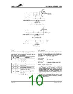
Power Down Operation - HALT
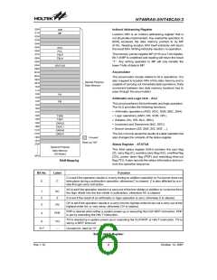
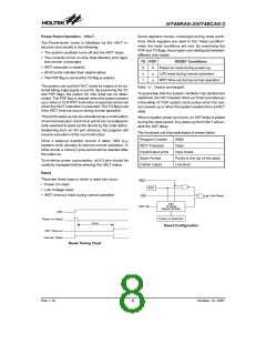
Some registers remain unchanged during reset condi-
tions. Most registers are reset to the ²initial condition²
when the reset conditions are met. By examining the
PDF and TO flags, the program can distinguish between
different chip resets.
The Power-down mode is initialised by the HALT in-
struction and results in the following:
·
The system oscillator turns off and the WDT stops.
·
The contents of the on-chip Data Memory and regis-
TO PDF
RESET Conditions
ters remain unchanged.
·
WDT prescaler is cleared.
0
u
1
0
u
u
Power-on reset during power-up
LVR reset during normal operation
WDT time-out during normal operation
·
All I/O ports maintain their original status.
·
The PDF flag is set and the TO flag is cleared.
The system can quit the HALT mode by means of an ex-
ternal falling edge signal on port B. By examining the TO
and PDF flags, the reason for chip reset can be deter-
mined. The PDF flag is cleared when the system powers
up or when a CLR WDT instruction is executed and is set
when the HALT instruction is executed. The TO flag is set
if the WDT time-out occurs during normal operation.
Note: ²u² means unchanged.
To guarantee that the system oscillator has started and
stabilized, the SST (System Start-up Timer) provides an
extra-delay of 1024 system clock pulses when the sys-
tem powers up or when the system awakes from a HALT
state.
The port B wake-up can be considered as a continuation
of normal execution. Each bit in port B can be independ-
ently selected to wake up the device by the code option.
Awakening from an I/O port stimulus, the program will
resume execution of the next instruction.
When a system power up occurs, an SST delay is added
during the reset period. Any wake-up from HALT will en-
able the SST delay.
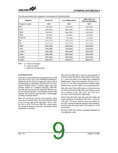
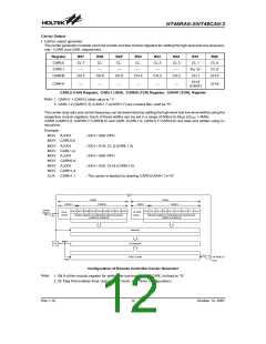
The functional unit chip reset status is shown below.
Program Counter
WDT Prescaler
Input/Output ports
Stack Pointer
000H
Once a wake-up event(s) occurs, it takes 1024 tSYS
(system clock periods) to resume normal operation. In
other words, a dummy cycle period will be inserted after
the wake-up.
Clear
Input mode
Points to the top of the stack
Low level
To minimize power consumption, all I/O pins should be
carefully managed before entering the HALT status.
Carrier output
Reset
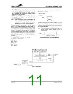
There are three ways in which a reset can occur:
H
A
L
T
·
Power On reset
W
D
T
·
Low Voltage reset
·
WDT time-out reset during normal operation
C
o
l
d
R
e
s
e
t
L
V
R
S
S
T
O
S
C
1
1
0
-
s
t
a
g
e
R
i
p
p
l
e
C
o
u
n
t
e
r
V
D
D
P
o
w
e
r
-
o
n
D
e
t
e
c
t
i
o
n
P
o
w
e
r
-
o
n
R
e
s
e
t
t
R S T D
Reset Configuration
S
S
T
T
i
m
e
-
o
u
t
I
n
t
e
r
n
a
l
R
e
s
e
t
Reset Timing Chart
Rev.1.10
8
October 12, 2007

 HOLTEK [ HOLTEK SEMICONDUCTOR INC ]