HT48RA0-3/HT48CA0-3
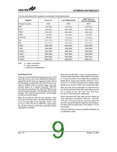
The chip reset status of the registers is summarised in the following table:
WDT Time-out
Register
Power On
Low Voltage Reset
(Normal Operation)
Program Counter
MP
000H
000H
000H
-xxx xxxx
xxxx xxxx
xxxx xxxx
--xx xxxx
-uuu uuuu
uuuu uuuu
uuuu uuuu
--uu uuuu
--uu uuuu
1111 1111
1111 1111
0000 0000
1000 0000
0000 0000
0000 0000
0000 0000
0000 0010
-uuu uuuu
uuuu uuuu
uuuu uuuu
--uu uuuu
ACC
TBLP
TBLH
STATUS
PA
--00 xxxx
1111 1111
1111 1111
0000 0000
1000 0000
0000 0000
0000 0000
0000 0000
0000 0010
--1u uuuu
1111 1111
1111 1111
0000 0000
1000 0000
0000 0000
0000 0000
0000 0000
0000 0010
PB
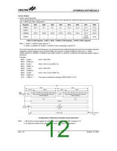
TSR0
TSR1
CARL0
CARL1
CARH0
CARH1
Note:
²u² means unchanged
²x² means unknown
²-² stands for unimplemented
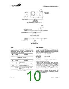
Input/Output Ports
When PA and PB0~PB1 is used for input operation, it
should be noted that before reading data from the pads,
a ²1² should be written to the related bits to disable the
NMOS device. That is, the instruction ²SET [m].i² (i=0~7
for PA, i=0~1 for PB) is executed first to disable related
NMOS device, and then ²MOV A, [m]² to get stable data.
There are an 8-bit bidirectional input/output port, a 6-bit
input with 2-bit I/O port in the HT48RA0-3/HT48CA0-3,
labeled PA and PB which are mapped to [12H], [14H] of
the Data Memory, respectively. Each bit of PA can be se-
lected as NMOS output or Schmitt trigger input with
pull-high resistor by a software instruction. PB0~PB1
have the same structure as PA, while PB2~PB6 can only
be used for input operation - Schmitt trigger with pull-high
resistors. PB7 is used for input operation - Schmitt trigger
but without pull-high resistor.
After chip reset, PA and PB remain at a high level input
line. Each bit of PA and PB0~PB1 output latches can be
set or cleared by the ²SET [m].i² and ²CLR [m].i²
(m=12H or 14H) instructions respectively.
Some instructions first input data and then follow the
output operations. For example, ²SET [m].i², ²CLR [m]²,
²CPL [m]², ²CPLA [m]² read the entire port states into
the CPU, execute the defined operations (bit-operation),
and then write the results back to the latches or to the
accumulator.
When PA and PB are used for input operation, these
ports are non-latched, that is, the inputs should be ready
at the T2 rising edge of the instruction ²MOV A, [m]²
(m=12H or 14H). For PA and PB0~PB1 output opera-
tion, all data is latched and remains unchanged until the
output latch is rewritten.
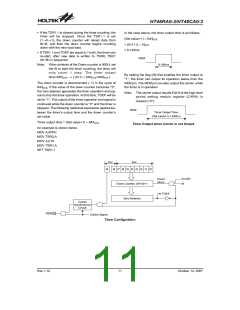
Each line of PB has a wake-up capability selectable via
a configuration option.
Rev.1.10
9
October 12, 2007

 HOLTEK [ HOLTEK SEMICONDUCTOR INC ]