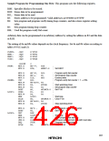
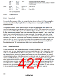
CMP.B
BEQ
BRA
#H'32,
NGEND
PRGMS
R6L
; Program-verify executed 50 times?
; If program-verify executed 50 times, branch to NGEND
; Program again
PVOK:
BCLR
MOV.B
MOV.B
#2,
#H'00,
R6L,
@FLMCR:8 ; Clear PV bit
R6L
;
@EBR*:8
; Clear EBR*
One byte programmed
Programming error
NGEND:
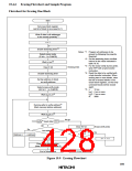
19.4.4 Erase Mode
To erase the flash memory, follow the erasing flowchart shown in figure 19.9. This erasing flow
can erase data without subjecting the device to voltage stress or impairing the reliability of
programmed data.
To erase flash memory, before starting to erase, first place all memory data in all blocks to be
erased in the programmed state (program all memory data to H'00). If all memory data is not in the
programmed state, follow the sequence described later (figure 19.10) to program the memory data
to zero. Select the flash memory areas to be erased with erase block registers 1 and 2 (EBR1 and
EBR2). Next set the E bit in FLMCR, selecting erase mode. The erase time is the time during
which the E bit is set. To prevent overerasing, use a software timer to divide the erase time into
repeated 10 ms intervals, and perform erase operations a maximum of 3000 times so that the total
erase time does not exceed 30 seconds. Overerasing, due to program runaway for example, can
give memory cells a negative threshold voltage and cause them to operate incorrectly. Before
selecting erase mode, set up the watchdog timer so as to prevent overerasing.
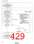
19.4.5 Erase-Verify Mode
In erase-verify mode, after data has been erased, it is read to check that it has been erased
correctly. After the erase time has elapsed, exit erase mode (clear the E bit to 0) and select erase-
verify mode (set the EV bit to 1). Before reading data in erase-verify mode, write H'FF dummy
data to the address to be read. This dummy write applies an erase-verify voltage to the memory
cells at the latched address. If the flash memory is read in this state, the data at the latched address
will be read. After the dummy write, wait 2 µs or more before reading. When performing the
initial dummy write, wait 4 µs or more after selecting erase-verify mode. If the read data has been
successfully erased, perform an erase-verify (dummy write, wait 2 µs or more, then read) for the
next address. If the read data has not been erased, select erase mode again and repeat the same
erase and erase-verify sequence through the last address, until all memory data has been erased to
1. Do not repeat the erase and erase-verify sequence more than 3000 times, however.
398

 HITACHI [ HITACHI SEMICONDUCTOR ]