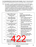
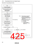
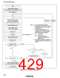
19.4.3 Programming Flowchart and Sample Program
Flowchart for Programming One Byte
Start
Set erase block register
(set bit of block to be programmed to 1)
Write data to flash memory (flash
memory latches write
address and data)*1
n = 1
Enable watchdog timer*2
Select program mode
Notes: *1 Write the data to be programmed
(P bit = 1 in FLMCR)
with a byte transfer instruction.
*2 Set the timer overflow interval to the
shortest value (CKS2, CKS1, CKS0
all cleared to 0).
Wait (x) µs*4
*3 Read the memory data to be verified
with a byte transfer instruction.
Clear P bit
End of programming
*4 x:
tVS1: 4 µs or more
N: 50 (set N so that total
10 to 20 µs
Disable watchdog timer
Select program-verify mode
(PV bit = 1 in FLMCR)
programming time does not
exceed 1 ms)
Wait (tVS1) µs*4
No go
Verify*3 (read memory)
OK
End of verification
Clear PV bit
Clear PV bit
Clear erase block register
(clear bit of programmed block to 0)
No
n ≥ N?*4
End (1-byte data programmed)
Yes
n + 1 → n
Programming error
Figure 19.8 Programming Flowchart
396

 HITACHI [ HITACHI SEMICONDUCTOR ]