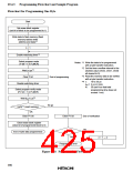
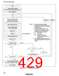
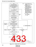
Prewrite Flowchart
Start
Set erase block register
(set bit of block to be programmed to 1)
Set start address*5
n = 1
Write H'00 to flash memory
(Flash memory latches
write address and write data)*1
Address + 1 → address
Notes: *1 Use a byte transfer instruction.
Enable watchdog timer*2
*2 Set the timer overflow interval to the
shortest value (CKS2, CKS1, CKS0
all cleared to 0).
*3 In prewrite-verify mode P, E, PV,
and EV are all cleared to 0 and 12 V
is applied to FVPP. Read the data
with a byte transfer instruction.
Select program mode
( P bit = 1 in FLMCR)
Wait (x) µs*4
*4 x:
tVS1: 4 µs or more
N: 50 (set N so that total
10 to 20 µs
End of programming
Clear P bit
Disable watchdog timer
programming time does not
exceed 1 ms)
*5 Start and last addresses shall be top
and last addresses of the block to be
erased.
Wait (tVS1) µs*4
Prewrite verify*3
No go
(read data = H'00?)
OK
No
n ≥ N?*4
Yes
n + 1 → n
Programming error
No
Last address?*5
Yes
Clear erase block register
(clear bit of programmed block to 0)
End of prewrite
Figure 19.10 Prewrite Flowchart
400

 HITACHI [ HITACHI SEMICONDUCTOR ]