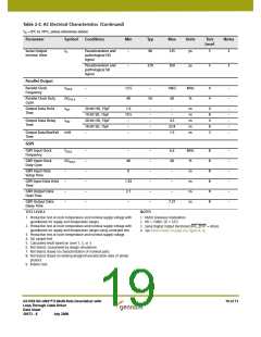
Table 2-2: AC Electrical Characteristics (Continued)
TA = 0°C to 70°C, unless otherwise shown
Parameter
Symbol
Conditions
Min
Typ
Max
Units
Test
Notes
Level
Serial Output
Intrinsic Jitter
tIJ
Pseudorandom and
pathological HD
signal
–
90
125
ps
5
3
Pseudorandom and
pathological SD
signal
–
270
350
ps
5
3
Parallel Output
Parallel Clock
Frequency
fPCLK
DCPCLK
tOH
–
–
13.5
40
–
148.5
60
MHz
%
4
4
–
–
Parallel Clock Duty
Cycle
50
Output Data Hold
Time
20-bit HD, 15pF
10-bit SD, 15pF
20-bit HD, 15pF
10-bit SD, 15pF
–
1.0
19.5
–
–
–
–
–
–
–
–
ns
ns
ns
ns
ns
4
8
4
8
3
–
–
–
–
–
Output Data Delay
Time
tOD
4.5
22.8
1.5
–
Output Data Rise/Fall
Time
tr/tf
–
GSPI
GSPI Input Clock
Frequency
fSCLK
–
–
–
–
–
–
–
40
0
–
–
–
–
–
–
6.6
60
–
MHz
%
8
8
8
8
8
8
–
–
–
–
–
–
GSPI Input Clock
Duty Cycle
DCSCLK
GSPI Input Data
Setup Time
–
–
–
–
ns
GSPI Input Data Hold
Time
1.43
2.1
–
–
ns
GSPI Output Data
Hold Time
–
ns
GSPI Output Data
Delay Time
7.27
ns
TEST LEVELS
NOTES
1. Production test at room temperature and nominal supply voltage with
guardbands for supply and temperature ranges.
2. Production test at room temperature and nominal supply voltage with
guardbands for supply and temperature ranges using correlated test.
3. Production test at room temperature and nominal supply voltage.
4. QA sample test.
1. 6MHz sinewave modulation.
2. HD = 1080i, SD = 525i
3. Serial Digital Output Reclocked (RC_BYP = HIGH).
4. See Device Reset on page 64, Figure 4-16.
5. Calculated result based on Level 1, 2, or 3.
6. Not tested. Guaranteed by design simulations.
7. Not tested. Based on characterization of nominal parts.
8. Not tested. Based on existing design/characterization data of similar
product.
9. Indirect test.
GS1559 HD-LINX™ II Multi-Rate Deserializer with
Loop-Through Cable Driver
Data Sheet
19 of 71
30572 - 8
July 2008

 GENNUM [ GENNUM CORPORATION ]