FA13842, 13843, 13844, 13845
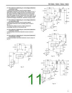
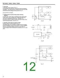
Fig. 22 illustrates a case when the inductor current variation
Converge
∆ i
L
’ at t1 is smaller than ∆ i at t0. In this case, inductor current
L
variations gradually converges and the inductor current
becomes stable.
∆iL
∆iL´
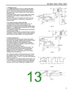
It is necessary to apply slope compensation to the control
signals in order to prevent such subharmonic oscillations when
the inductor current is continuous and the duty cycle is greater
than 50%.
to
t1
Fig. 22
The waveform of the inductor current when slope
compensation is applied is shown in Fig. 23.
Slope compensation adds the negative slope of inclination
–Kc to the control signal of the inductor peak current.
∆ iL’ shows the variation of the inductor current at t1 when
Is
-Kc
slope compensation is not applied, and ∆ i ’ s shows the
L
∆iL´
variation of the inductor current at t1 when slope compensation
is applied.
Lu
∆iL
-Ld
Thus, ∆ i
when –Kc is large. It is necessary to apply slope
compensation to satisfy the equation ∆ i ≥ ∆ i ’s, that is,
L
’ can be changed by –Kc, and ∆ I ’ s becomes smaller
L
∆iL´s
L
L
Compensated
I –Kc I ≥ I –1/2 Ld I as the condition which achieves stable
operation.
Ton
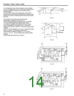
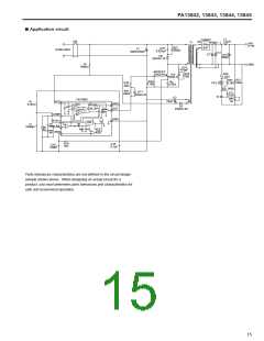
Typical circuits are shown in Fig. 24 and 25.
T
to
t1
Fig. 23
Vin
Vcc
VCC
7
VREF
8
UVLO
Vcc
5VREF
RT
ENB
2.5V
OUT
30V
UVLO
OUTPUT
Tr7
6
ENB
R18
CT
R27
Rs
Output
C10
RT/CT
5
GND
4
OSC
R25
R24
ER AMP
2R
1R
FB
R26 C13
COMP
2
1V
S
1
3
Q
FF
R
QB
ISNS
Fig. 24
Vin
Vcc
VCC
7
VREF
UVLO
Vcc
8
5VREF
RT
ENB
2.5V
OUT
30V
UVLO
OUTPUT
ENB
Tr7
6
R18
CT
R27
Rs
Output
C10
RT/CT
5
GND
4
OSC
R25
R24
ER AMP
2R
1R
FB
2
R26 C13
COMP
1V
S
1
3
Q
FF
R
QB
ISNS
Fig. 25
14

 FUJI [ FUJI ELECTRIC ]