FA13842, 13843, 13844, 13845
DB
~
T1
+
5. Output stage
An output stage of CMOS inverter composition is incorporated,
thereby making it possible to fully swing the gate voltage of a
+
AC INPUT
C1
power MOSFET to the VCC
.
The output stage provides a source current of 400mA and a
sink current of 1A as the peak current capacity. (When VCC is
15V)
~
R1
The output stage is held in the “Low” state in standby mode.
D1
+
C2
6. Reference voltage
7
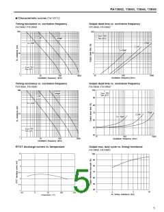
The 5.0V(±5%) bandgap reference(Tj=25˚C) is built-in.
It is possible to supply a current of about 10mA to an external
circuit in addition to supplying a charge current to the timing
capacitor of the oscillator. (See characteristic curve on page
46.)
FA13842
MOSFET
Rs
6
Connect a ceramic bypass capacitor of 0.1µF or higher to the
VREF terminal to stabilize this voltage.
Fig. 4
Input:100V AC
C2=47µF
4
C2=22µF
■ Design advice
3
2
1
0
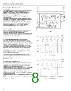
1. Start-up circuit
A typical start-up circuit is shown in Fig. 4.
The AC INPUT voltage charges capacitor C2 and supplies
start-up current to the IC through start-up resistance R1. When
this voltage reaches the ON threshold voltage, the IC reverts to
the operation mode and electric power is supplied from the
bias winding of the transformer thereafter.
C2=10µF
0
200
400
600
800
1000
1200
Start-up resistance R1 (kΩ)
Using CMOS process, the start-up current is less than 30µA.
Fig. 5 Start-up time
When the start-up resistance is increased, the charging rate of
capacitor C2 decreases and start-up time increases. Select
the optimum values for R1 and C2.
The relation between the start-up resistance and start-up time
for the circuit indicated in Fig. 4 is shown in Fig. 5.
Fig. 6 indicates a method to increase the start-up resistance to
reduce loss and shorten start-up time. The start-up time is
shortened by reducing the capacitance of C2. The bias current
is supplied from C3 after start-up.
R1
D1
D2
+
+
C2
C3
7
FA13842
6
2. Synchronized operation with external signals
The circuit shown in Fig. 7 allows synchronized operation with
external signals.
Fig. 6
Synchronized operation is started when the RT/CT terminal
voltage is raised to about 3V or higher. (Synchronized at
leading edge.)
The external synchronizing signal should be higher than the
free-run frequency.
8
REF
In the case of FA13844/45, the output frequency of the OUT
terminal is 1/2 that of the synchronizing signal frequency.
RT
Synchronized
4
OSC
CT
C4
2R
+
R2
2
1
ER AMP
D3
1R
5
Fig. 7
9

 FUJI [ FUJI ELECTRIC ]