FA13842, 13843, 13844, 13845
D6
DB
~
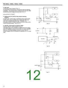
3-1 The method of detecting an overvoltage (detection
on primary side)
T1
+
+
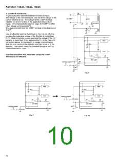
A typical latched shutdown circuit to protect against
overvoltages detected on the primary side is shown in Fig. 11.
When the secondary voltage increases in the flyback circuit,
the voltage of the bias winding also increases in proportion.
When this voltage increase is detected by zener diode ZD1, a
latched shutdown is accomplished. As the secondary voltage
is detected through a transformer, detection accuracy is low.
C7
+
AC INPUT
C1
~
R1
D1
R9
+
R6
C2
7
ZD2
MOSFET
Rs
FA13842
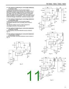
3-2 The method of detecting an overvoltage (detection
on secondary side)
A typical latched shutdown circuit to protect against
overvoltages detected on the secondary side is shown in
Fig. 12.
6
PC1
1
R8
R4
Tr2
The detected voltage accuracy is high compared to
overvoltage detection on the primary side.
D5
PC1
R7
Tr1
R3
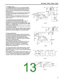
3-3 The method of detecting an overcurrent (detection
of primary current)
C6
Fig. 12
A typical primary overcurrent detection circuit is shown in
Fig. 13.
DB
T1
~
~
+
3-4 The method of detecting an overcurrent (detection
of secondary current)
A typical secondary overcurrent detection circuit is shown in
Fig. 14.
+
AC INPUT
C1
R1
D1
C2
+
R6
7
DB
~
T1
+
MOSFET
R12
FA13842
6
1
3
+
AC INPUT
C1
D5
~
R4
Rs
R1
Tr2
R11
D1
C2
Tr1
Tr3
+
R3
R6
R10
C6
7
C8
ZD1
Tr2
MOSFET
Rs
Fig. 13
FA13842
6
1
D6
R13
DB
~ +
T1
R4
D5
+
+
AC INPUT
Tr4
C1
C7
Tr1
~
R3
C6
R1
R14
PC1
D1
Fig. 11
+
R6
C2
7
R15
MOSFET
Rs
FA13842
6
Tr5
1
R16
R8
R4
Tr2
C6
D5
PC1
R7
Tr1
R3
Fig. 14
11

 FUJI [ FUJI ELECTRIC ]