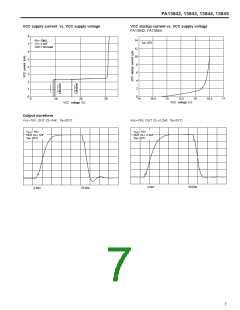
FA13842, 13843, 13844, 13845
7. Feedback circuit
D6
T1
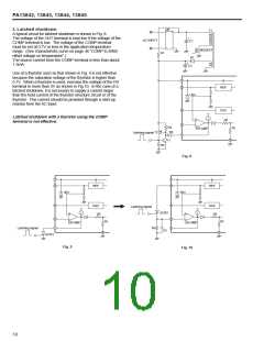
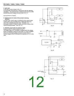
7-1 A method that does not use an internal ER AMP
A method that does not use an internal ER AMP is shown in
Fig. 18. Connect the FB terminal to GND and connect an
optocoupler to the COMP terminal of the ER AMP output for
feedback control.
It is possible to obtain a precise power supply output voltage,
because the output voltage is monitored directly on the
secondary side.
+
+
C1
C7
MOSFET
R20
1
2
C11
R19
R21
R23
2R
PC2
Rs
PC2
R22
+
2.5V
R
Be sure to connect the FB terminal to the GND in this case.
There is the possibility of a malfunction occuring if the FB
terminal is open.
+
3
R18
C12
C10
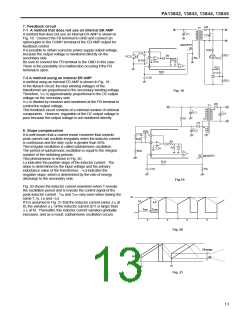
7-2 A method using an internal ER AMP
A method using an internal ER AMP is shown in Fig. 19.
In the flyback circuit, the bias winding voltages of the
transformer are proportional to the secondary winding voltage.
Therefore, VCC is approximately proportional to the DC output
voltage on the secondary side.
Fig. 18
V
CC is divided by resistors and monitored at the FB terminal to
D6
T1
control the output voltage.
This feedback circuit consists of a minimal number of external
components. However, regulation of the DC output voltage is
poor because the output voltage is not monitored directly.
+
+
C1
C7
R1
D1
+
C2
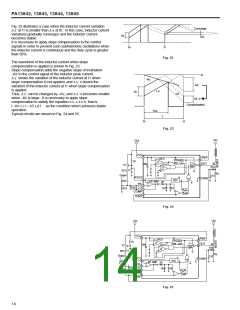
8. Slope compensation
R26
C13
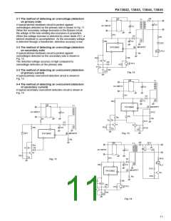
It is well known that a current mode converter that controls
peak current can oscillate irregularly when the inductor current
is continuous and the duty cycle is greater than 50%.
This irregular oscillation is called subharmonic oscillation.
The period of subharmonic oscillation is equal to the integral
number of the switching periods.
1
2
R25
2R
+
2.5V
R
R24
+
3
MOSFET
Rs
This phenomenon is shown in Fig. 20.
R18
Lu indicates the positive slope of the inductor current. The
slope is determined by the input voltage and the primary
inductance value of the transformer. –Ld indicates the
negative slope, which is determined by the rate of energy
discharge to the secondary side.
C10
Fig.19
Fig. 20 shows the inductor current waveform when T reveals
the oscillation period and Is reveals the control signal of the
peak inductor current. TON and TOFF vary even when having the
same T, Is, Lu and –Ld.
Is
Lu
-Ld
If it is assumed in Fig. 21 that the inductor current varies ∆ i
t0, the variation ∆ iL’ of the inductor current at t1 is larger than
∆ i at t0. Thereafter, this inductor current variation gradually
increases, and as a result, subharmonic oscillation occurs.
L
at
TON
TOFF
L
T
T
T
T
Fig. 20
Diverge
∆iL
∆iL´
t1
to
Fig. 21
13

 FUJI [ FUJI ELECTRIC ]