FA13842, 13843, 13844, 13845
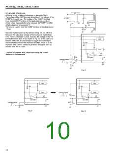
Vin
Vcc
■ Description of each circuit
1. Oscillator
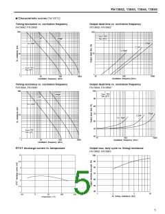
The oscillation frequency is determined by timing resistance R
T
and timing capacitor C , which are connected to RT/CT
T
terminal. CT is charged to about 3V through RT from a 5V
reference, and discharged to about 1.4V by the built-in
discharge circuit. (See Fig. 1, 2, 3.)
VCC
7
VREF
OUT
UVLO
UVLO
VCC
ENB
8
5V REF
2.5V
Blanking pulses are generated in the IC during the C
T
30V
OUTPUT
ENB
6
discharge period.
The output is fixed in the “low” state by these pulses, and a
fixed dead time is produced. See the characteristic curves on
RT
RS
page 45 for the oscillation frequency, R
T
and C .
T
5
GND
In the case of FA13844/45, a flip-flop causes the output to be
blanked with every other cycle. Therefore, the switching
frequency of a power MOSFET is 1/2 of the oscillation
RT/CT
4
2
OSC
ER AMP
CT
2R
FB
frequency determined by R
T
and C
T
. (See Fig. 3.)
S
1R
1V
Q
FF
1
3
COMP
QB
R
ISNS
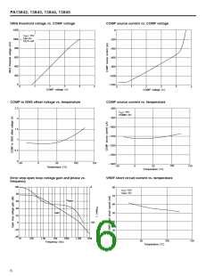
2. Error amplifier
Inverting input and output are connected to the FB terminal
and COMP terminal, respectively. A 2.5V reference is
connected internally to the non-inverting input.
Fig. 1
The output voltage is offset by a diode V voltage (=0.7V) and
F
divided by three. The divided voltage is connected to the input
of the current sensing comparator.
3V
CT
1.4V
3. Current sensing comparator and PWM latch
The “High” state of the OUT terminal begins at the time C
Set
T
starts charging. The OUT terminal turns to “Low” when the
peak inductor current reaches the threshold level controlled by
the error amplifier output (COMP terminal).
COMP
ISENS
The inductor current is converted to a voltage by sensing
resistor R inserted between GND and the source of a power
S
MOSFET. This voltage is monitored by the ISNS terminal.
Reset
The peak current of inductor “Ipk” is expressed as follows:
Ipk=(Vcomp–0.7) / (3•RS)
0.7V
VF
OUT
Vcomp: a voltage on COMP terminal
The maximum value of the threshold level of the current
sensing comparator is held to 1V. Therefore, the maximum
peak current “Ipk(max)” is as follows:
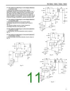
Fig. 2 FA13842, 13843
Ipk(max)=1.0V/R
S
3V
CT
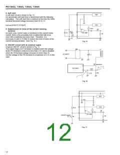
4. Undervoltage lockout (UVLO)
1.4V
In order to set the IC in the operation mode before the output
stage(OUT terminal) is enabled, two under-voltage lockout
comparators are incorporated to monitor the power supply
voltage (VCC) and reference voltage (VREF).
Set
The threshold level of the VCC comparator is set at 16.5V/9V for
FA13842/44 and 9.6V/9V for FA13843/45. In the standby
mode, in which the VCC is under ON threshold, the power
supply current is maintained at nearly 0 (zero). However, a
maximum current of 30µA is required to change from standby
mode to operating mode .
COMP
ISENS
Reset
The threshold level of the VREF comparator is set at about 3.2V/
2.0V.
OUT
A 30V zener diode is connected to VCC and GND to protect the
IC against overvoltages.
Fig. 3 FA13844, 13845
8

 FUJI [ FUJI ELECTRIC ]