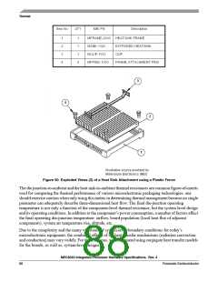
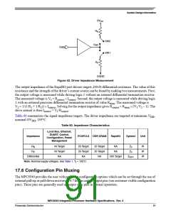
System Design Information
While HRESET is asserted however, these pins are treated as inputs. The value presented on these pins
while HRESET is asserted, is latched when HRESET deasserts, at which time the input receiver is disabled
and the I/O circuit takes on its normal function. Most of these sampled configuration pins are equipped
with an on-chip gated resistor of approximately 20 kΩ. This value should permit the 4.7-kΩ resistor to pull
the configuration pin to a valid logic low level. The pull-up resistor is enabled only during HRESET (and
for platform/system clocks after HRESET deassertion to ensure capture of the reset value). When the input
receiver is disabled the pull-up is also, thus allowing functional operation of the pin as an output with
minimal signal quality or delay disruption. The default value for all configuration bits treated this way has
been encoded such that a high voltage level puts the device into the default state and external resistors are
needed only when non-default settings are required by the user.
Careful board layout with stubless connections to these pull-down resistors coupled with the large value
of the pull-down resistor should minimize the disruption of signal quality or speed for output pins thus
configured.
The platform PLL ratio and e500 PLL ratio configuration pins are not equipped with these default pull-up
devices.
17.7 Pull-Up Resistor Requirements
The MPC8540 requires high resistance pull-up resistors (10 kΩ is recommended) on open drain type pins
2
including EPIC interrupt pins. I C open drain type pins should be pulled up with ~1 kΩ resistors.
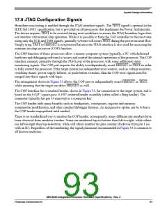
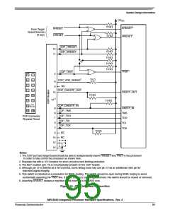
Correct operation of the JTAG interface requires configuration of a group of system control pins as
demonstrated in Figure 54. Care must be taken to ensure that these pins are maintained at a valid deasserted
state under normal operating conditions as most have asynchronous behavior and spurious assertion will
give unpredictable results.
TSEC1_TXD[3:0] must not be pulled low during reset. Some PHY chips have internal pulldowns that
could cause this to happen. If such PHY chips are used, then a pullup must be placed on these signals strong
enough to restore these signals to a logical 1 during reset.
Three test pins also require pull-up resistors (100 Ω - 1 kΩ). These pins are L1_TSTCLK, L2_TSTCLK,
and LSSD_MODE. These signals are for factory use only and must be pulled up to OVDD for normal
machine operation.
Refer to the PCI 2.2 specification for all pull-ups required for PCI.
MPC8540 Integrated Processor Hardware Specifications, Rev. 4
92
Freescale Semiconductor

 FREESCALE [ Freescale ]