System Design Information
17 System Design Information
This section provides electrical and thermal design recommendations for successful application of the
MPC8540.
17.1 System Clocking
The MPC8540includes two PLLs.
1. The platform PLL generates the platform clock from the externally supplied SYSCLK input. The
frequency ratio between the platform and SYSCLK is selected using the platform PLL ratio
configuration bits as described in Section 15.2, “Platform/System PLL Ratio.”
2. The e500 Core PLL generates the core clock as a slave to the platform clock. The frequency ratio
between the e500 core clock and the platform clock is selected using the e500 PLL ratio
configuration bits as described in Section 15.3, “e500 Core PLL Ratio.”
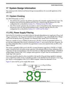
17.2 PLL Power Supply Filtering
Each of the PLLs listed above is provided with power through independent power supply pins (AV 1 and
DD
AV 2, respectively). The AV level should always be equivalent to V , and preferably these voltages
DD
DD
DD
will be derived directly from V through a low frequency filter scheme such as the following.
DD
There are a number of ways to reliably provide power to the PLLs, but the recommended solution is to
provide three independent filter circuits as illustrated in Figure 51, one to each of the three AV pins. By
DD
providing independent filters to each PLL the opportunity to cause noise injection from one PLL to the
other is reduced.
This circuit is intended to filter noise in the PLLs resonant frequency range from a 500 kHz to 10 MHz
range. It should be built with surface mount capacitors with minimum Effective Series Inductance (ESL).
Consistent with the recommendations of Dr. Howard Johnson in High Speed Digital Design: A Handbook
of Black Magic (Prentice Hall, 1993), multiple small capacitors of equal value are recommended over a
single large value capacitor.
Each circuit should be placed as close as possible to the specific AV pin being supplied to minimize
DD
noise coupled from nearby circuits. It should be possible to route directly from the capacitors to the AV
pin, which is on the periphery of the 783 FC-PBGA footprint, without the inductance of vias.
DD
Figure 51 shows the PLL power supply filter circuit.
10 Ω
VDD
AVDD (or L2AVDD)
2.2 µF
2.2 µF
Low ESL Surface Mount Capacitors
GND
Figure 51. PLL Power Supply Filter Circuit
MPC8540 Integrated Processor Hardware Specifications, Rev. 4
Freescale Semiconductor
89

 FREESCALE [ Freescale ]