System Design Information
17.3 Decoupling Recommendations
Due to large address and data buses, and high operating frequencies, the MPC8540 can generate transient
power surges and high frequency noise in its power supply, especially while driving large capacitive loads.
This noise must be prevented from reaching other components in the MPC8540 system, and the MPC8540
itself requires a clean, tightly regulated source of power. Therefore, it is recommended that the system
designer place at least one decoupling capacitor at each V , OV , GV , and LV pins of the
DD
DD
DD
DD
MPC8540. These decoupling capacitors should receive their power from separate V , OV , GV ,
DD
DD
DD
LV , and GND power planes in the PCB, utilizing short traces to minimize inductance. Capacitors may
DD
be placed directly under the device using a standard escape pattern. Others may surround the part.
These capacitors should have a value of 0.01 or 0.1 µF. Only ceramic SMT (surface mount technology)
capacitors should be used to minimize lead inductance, preferably 0402 or 0603 sizes.
In addition, it is recommended that there be several bulk storage capacitors distributed around the PCB,
feeding the V , OV , GV , and LV planes, to enable quick recharging of the smaller chip
DD
DD
DD
DD
capacitors. These bulk capacitors should have a low ESR (equivalent series resistance) rating to ensure the
quick response time necessary. They should also be connected to the power and ground planes through two
vias to minimize inductance. Suggested bulk capacitors—100–330 µF (AVX TPS tantalum or Sanyo
OSCON).
17.4 Connection Recommendations
To ensure reliable operation, it is highly recommended to connect unused inputs to an appropriate signal
level. Unused active low inputs should be tied to OV , GV , or LV as required. Unused active high
DD
DD
DD
inputs should be connected to GND. All NC (no-connect) signals must remain unconnected.
Power and ground connections must be made to all external V , GV , LV , OV , and GND pins of
DD
DD
DD
DD
the MPC8540.
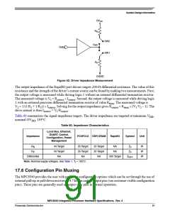
17.5 Output Buffer DC Impedance
The MPC8540 drivers are characterized over process, voltage, and temperature. There are two driver
2
types: a push-pull single-ended driver (open drain for I C) for all buses except RapidIO, and a
current-steering differential driver for the RapidIO port.
To measure Z for the single-ended drivers, an external resistor is connected from the chip pad to OV
0
DD
or GND. Then, the value of each resistor is varied until the pad voltage is OV /2 (see Figure 52). The
DD
output impedance is the average of two components, the resistances of the pull-up and pull-down devices.
When data is held high, SW1 is closed (SW2 is open) and R is trimmed until the voltage at the pad equals
P
OV /2. R then becomes the resistance of the pull-up devices. R and R are designed to be close to each
DD
P
P
N
other in value. Then, Z = (R + R )/2.
0
P
N
MPC8540 Integrated Processor Hardware Specifications, Rev. 4
90
Freescale Semiconductor

 FREESCALE [ Freescale ]