Freescale Semiconductor, Inc.
SECTION 7 SERIAL COMMUNICATIONS INTERFACE
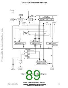
The serial communications interface (SCI) is a universal asynchronous receiver trans-
mitter (UART), one of two independent serial I/O subsystems in the MC68HC11F1
MCU. It has a standard nonreturn to zero (NRZ) format (one start bit, eight or nine data
bits, and one stop bit). Several baud rates are available. The SCI transmitter and re-
ceiver are independent, but use the same data format and bit rate.
7.1 Data Format
The serial data format requires the following conditions:
1. An idle-line in the high state before transmission or reception of a message.
2. A start bit, logic zero, transmitted or received, that indicates the start of each
character.
3. Data that is transmitted and received least significant bit (LSB) first.
4. A stop bit, logic one, used to indicate the end of a frame. (A frame consists of a
start bit, a character of eight or nine data bits, and a stop bit.)
5. A break (defined as the transmission or reception of a logic zero for some mul-
tiple number of frames).
Selection of the word length is controlled by the M bit of SCI control register SCCR1.
7.2 Transmit Operation
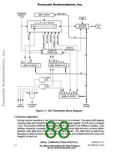
The SCI transmitter includes a parallel transmit data register (SCDR) and a serial shift
register. The contents of the serial shift register can only be written through the SCDR.
This double buffered operation allows a character to be shifted out serially while an-
other character is waiting in the SCDR to be transferred into the serial shift register.
The output of the serial shift register is applied to TxD as long as transmission is in
progress or the transmit enable (TE) bit of serial communication control register 2
(SCCR2) is set. The block diagram, Figure 7-1, shows the transmit serial shift register
and the buffer logic at the top of the figure.
SERIAL COMMUNICATIONS INTERFACE
TECHNICAL DATA
7-1
For More Information On This Product,
Go to: www.freescale.com

 FREESCALE [ Freescale ]