Freescale Semiconductor, Inc.
TRANSMITTER
BAUD RATE
CLOCK
(WRITE-ONLY)
SCDR Tx BUFFER
DDD1
10 (11) - BIT Tx SHIFT REGISTER
H (8) L
PIN BUFFER
AND CONTROL
PD1/
TxD
7
6
5
4
3
2
1
0
8
S
J
S
B
P
FORCE PIN
DIRECTION (OUT)
T
TRANSMITTER
CONTROL LOGIC
8
SCCR1 SCI CONTROL 1
SCSR INTERRUPT STATUS
8
TDRE
TIE
TC
8
TCIE
SCCR2 SCI CONTROL 2
SCI Rx
REQUESTS
SCI INTERRUPT
REQUEST
INTERNAL
DATA BUS
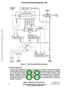
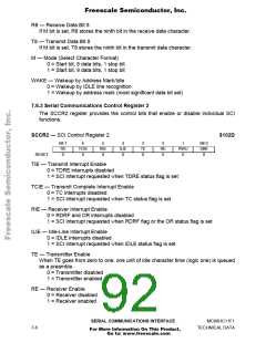
Figure 7-1 SCI Transmitter Block Diagram
7.3 Receive Operation
During receive operations, the transmit sequence is reversed. The serial shift register
receives data and transfers it to a parallel receive data register (SCDR) as a complete
word. This double buffered operation allows a character to be shifted in serially while
another character is already in the SCDR. An advanced data recovery scheme distin-
guishes valid data from noise in the serial data stream. The data input is selectively
sampled to detect receive data, and a majority voting circuit determines the value and
integrity of each bit.
SERIAL COMMUNICATIONS INTERFACE
MC68HC11F1
7-2
TECHNICAL DATA
For More Information On This Product,
Go to: www.freescale.com

 FREESCALE [ Freescale ]