Freescale Semiconductor, Inc.
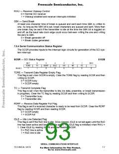
7.5 SCI Error Detection
Three error conditions, SCDR overrun, received bit noise, and framing can occur dur-
ing generation of SCI system interrupts. Three bits (OR, NF, and FE) in the serial com-
munications status register (SCSR) indicate if one of these error conditions exists.
The overrun error (OR) bit is set when the next byte is ready to be transferred from the
receive shift register to the SCDR and the SCDR is already full (RDRF bit is set). When
an overrun error occurs, the data that caused the overrun is lost and the data that was
already in SCDR is not disturbed. The OR is cleared when the SCSR is read (with OR
set), followed by a read of the SCDR.
The noise flag (NF) bit is set if there is noise on any of the received bits, including the
start and stop bits. The NF bit is not set until the RDRF flag is set. The NF bit is cleared
when the SCSR is read (with FE equal to one) followed by a read of the SCDR.
When no stop bit is detected in the received data character, the framing error (FE) bit
is set. FE is set at the same time as the RDRF. If the byte received causes both fram-
ing and overrun errors, the processor only recognizes the overrun error. The framing
error flag inhibits further transfer of data into the SCDR until it is cleared. The FE bit is
cleared when the SCSR is read (with FE equal to one) followed by a read of the SCDR.
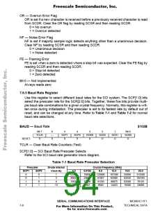
7.6 SCI Registers
There are five addressable registers associated with the SCI. SCCR1, SCCR2, and
BAUD are control registers. SCDR is the SCI data register and SCSR is the SCI status
register. Refer to the BAUD register description as well as the block diagram for the
baud rate generator.
7.6.1 Serial Communications Data Register
SCDR is a parallel register that performs two functions. It is the receive data register
when it is read, and the transmit data register when it is written. Reads access the re-
ceive data buffer and writes access the transmit data buffer. Receive and transmit are
double buffered.
SCDR — SCI Data Register
$102F
Bit 7
R7/T7
I
6
R6/T6
I
5
R5/T5
I
4
R4/T4
I
3
R3/T3
I
2
R2/T2
I
1
R1/T1
I
Bit 0
R0/T0
I
RESET:
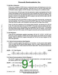
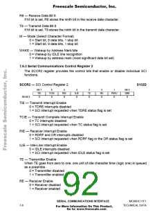
7.6.2 Serial Communications Control Register 1
The SCCR1 register provides the control bits that determine word length and select
the method used for the wakeup feature.
SCCR1 — SCI Control Register 1
$102C
Bit 7
R8
I
6
T8
I
5
—
0
4
M
0
3
WAKE
0
2
—
0
1
—
0
Bit 0
—
RESET:
0
SERIAL COMMUNICATIONS INTERFACE
TECHNICAL DATA
7-5
For More Information On This Product,
Go to: www.freescale.com

 FREESCALE [ Freescale ]