Freescale Semiconductor, Inc.
impedance state, as neither the N-channel nor the P-channel devices are active. It is
customary to have an external pull-up resistor on lines that are driven by open-drain
devices. Port C can only be configured for wired-OR operation when the MCU is in sin-
gle-chip or bootstrap modes.
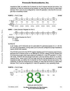
PORTC — Port C Data
$1006
Bit 7
PC7
6
5
4
3
2
1
Bit 0
PC0
PC6
PC5
PC4
PC3
PC2
PC1
S. Chip or
Boot:
PC7
I
PC6
I
PC5
I
PC4
I
PC3
I
PC2
I
PC1
I
PC0
I
RESET:
Expan. or
Test: DATA7
DATA6
DATA5
DATA4
DATA3
DATA2
DATA1
DATA0
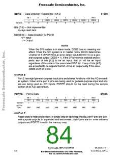
DDRC — Data Direction Register for Port C
$1007
Bit 7
DDC7
0
6
DDC6
0
5
DDC5
0
4
DDC4
0
3
DDC3
0
2
DDC2
0
1
DDC1
0
Bit 0
DDC0
0
RESET:
DDC[7:0] — Data Direction for Port C
0 = Input
1 = Output
6.4 Port D
In all modes, port D bits [5:0] can be used either for general-purpose I/O, or with the
SCI and SPI subsystems. During reset, port D pins are configured as high impedance
inputs (DDRD bits cleared).
The DWOM control bit in the SPCR register disables port D’s P-channel output drivers.
Because the N-channel driver is not affected by DWOM, setting DWOM causes port
D to become an open-drain-type output port suitable for wired-OR operation. In wired-
OR mode, (PORTD bits are at logic level zero), pins are actively driven low by the N-
channel driver. When a port D bit is at logic level one, the associated pin is in a high-
impedance state, as neither the N-channel nor the P-channel devices are active. It is
customary to have an external pull-up resistor on lines that are driven by open-drain
devices. Port D can be configured for wired-OR operation in any operating mode.
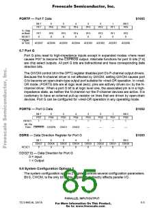
PORTD — Port D Data
$1008
Bit 7
—
6
—
0
5
PD5
I
4
PD4
I
3
PD3
I
2
PD2
I
1
PD1
I
Bit 0
PD0
I
RESET:
0
Alt. Pin
Func.:
—
—
SS
SCK
MOSI
MISO
TxD
RxD
PARALLEL INPUT/OUTPUT
TECHNICAL DATA
6-3
For More Information On This Product,
Go to: www.freescale.com

 FREESCALE [ Freescale ]