Freescale Semiconductor, Inc.
PORTF — Port F Data
$1005
Bit 7
PF7
6
5
4
3
2
1
Bit 0
PF0
PF6
PF5
PF4
PF3
PF2
PF1
S. Chip
or Boot:
PF7
0
PF6
0
PF5
0
PF4
0
PF3
0
PF2
0
PF1
0
PF0
0
RESET:
Expan.
or Test:
ADDR7
ADDR6
ADDR5
ADDR4
ADDR3
ADDR2
ADDR1
ADDR0
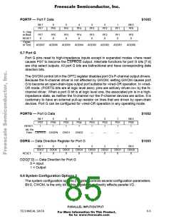
6.7 Port G
Port G pins reset to high-impedance inputs except in expanded modes where reset
causes PG7 to become the CSPROG output. Alternate functions for port G bits [7:4]
are chip select outputs. All port G bits are bidirectional and have corresponding data
direction bits.
The GWOM control bit in the OPT2 register disables port G's P-channel output drivers.
Because the N-channel driver is not affected by GWOM, setting GWOM causes port
G to become an open-drain-type output port suitable for wired-OR operation. In wired-
OR mode, (PORTG bits are at logic level zero), pins are actively driven low by the N-
channel driver. When a port G bit is at logic level one, the associated pin is in a high-
impedance state, as neither the N-channel nor the P-channel devices are active. It is
customary to have an external pull-up resistor on lines that are driven by open-drain
devices. Port G can be configured for wired-OR operation in any operating mode.
PORTG — Port G Data
$1002
Bit 7
PG7
I
6
PG6
I
5
PG5
I
4
PG4
I
3
PG3
I
2
PG2
I
1
PG1
I
Bit 0
PG0
I
RESET:
Alt. Pin
Func.: CSPROG CSGEN
CSIO1
CSIO2
—
—
—
—
DDRG — Data Direction Register for Port G
$1003
Bit 7
DDG7
0
6
DDG6
0
5
DDG5
0
4
DDG4
0
3
DDG3
0
2
DDG2
0
1
DDG1
0
Bit 0
DDG0
0
RESET:
DDG[7:0] — Data Direction for Port G
0 = Input
1 = Output
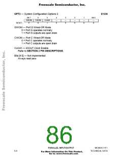
6.8 System Configuration Options 2
The system configuration options 2 register controls several configuration parameters.
Bit 6, CWOM, is the only bit in this register that directly affects parallel I/O.
PARALLEL INPUT/OUTPUT
TECHNICAL DATA
6-5
For More Information On This Product,
Go to: www.freescale.com

 FREESCALE [ Freescale ]