Freescale Semiconductor, Inc.
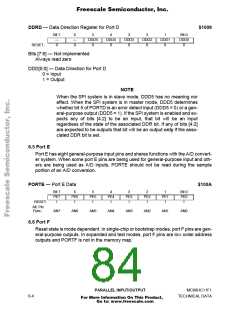
DDRD — Data Direction Register for Port D
$1009
Bit 7
—
6
—
0
5
DDD5
0
4
DDD4
0
3
DDD3
0
2
DDD2
0
1
DDD1
0
Bit 0
DDD0
0
RESET:
0
Bits [7:6] — Not implemented
Always read zero
DDD[5:0] — Data Direction for Port D
0 = Input
1 = Output
NOTE
When the SPI system is in slave mode, DDD5 has no meaning nor
effect. When the SPI system is in master mode, DDD5 determines
whether bit 5 of PORTD is an error detect input (DDD5 = 0) or a gen-
eral-purpose output (DDD5 = 1). If the SPI system is enabled and ex-
pects any of bits [4:2] to be an input, that bit will be an input
regardless of the state of the associated DDR bit. If any of bits [4:2]
are expected to be outputs that bit will be an output only if the asso-
ciated DDR bit is set.
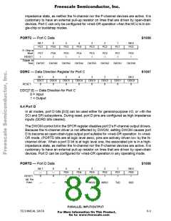
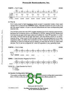
6.5 Port E
Port E has eight general-purpose input pins and shares functions with the A/D convert-
er system. When some port E pins are being used for general-purpose input and oth-
ers are being used as A/D inputs, PORTE should not be read during the sample
portion of an A/D conversion.
PORTE — Port E Data
$100A
Bit 7
PE7
I
6
PE6
I
5
PE5
I
4
PE4
I
3
PE3
I
2
PE2
I
1
PE1
I
Bit 0
PE0
I
RESET:
Alt. Pin
Func.:
AN7
AN6
AN5
AN4
AN3
AN2
AN1
AN0
6.6 Port F
Reset state is mode dependent. In single-chip or bootstrap modes, port F pins are gen-
eral-purpose outputs. In expanded and test modes, port F pins are low order address
outputs and PORTF is not in the memory map.
PARALLEL INPUT/OUTPUT
MC68HC11F1
6-4
TECHNICAL DATA
For More Information On This Product,
Go to: www.freescale.com

 FREESCALE [ Freescale ]