Freescale Semiconductor, Inc.
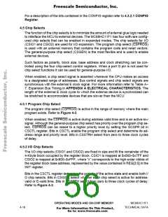
$0000
0000 PSIZ[A:B] = 0:0
64K
$1000
$8000
x000
x05F
x060
x7FF
x800
xFFF
96-BYTE REGISTER
BLOCK
PROGRAM CHIP SELECT
(CSPROG)
REMAPPABLE TO
4-KBYTE BOUNDARY
I/O CHIP SELECT 1
(CSIO1)
I/O CHIP SELECT 2
(CSIO2)
PSIZ[A:B] = 0:1
8000 32K
$C000
$E000
PSIZ[A:B] = 1:0
C000 16K
PSIZ[A:B] = 1:1
E000 8K
FFC0
VECTORS
$FE00
$FFFF
FFFF
FFFF
EXPANDED
MODE
Figure 4-3 Address Map for I/O and Program Chip Selects
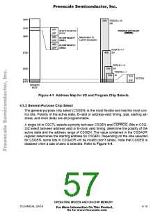
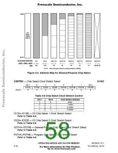
4.5.3 General-Purpose Chip Select
The general-purpose chip select (CSGEN) is the most flexible and has the most con-
trol bits. Polarity of the active state, E-valid or address-valid timing, size, starting ad-
dress, and clock delay are all programmable.
A single bit in CSCTL selects a priority between CSGEN and CSPROG. Bits in CSG-
SIZ select between address valid or E-clock valid timing, determine the polarity of the
active state and the address range of CSGEN. The value contained in the CSGADR
register determines the starting address for CSGEN. Depending on the size selected
for CSGEN, some bits in CSGADR will be invalid (don’t cares). Note that CSGEN is
disabled when a size of zero is selected. Refer to Figure 4-4.
OPERATING MODES AND ON-CHIP MEMORY
TECHNICAL DATA
4-19
For More Information On This Product,
Go to: www.freescale.com

 FREESCALE [ Freescale ]