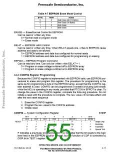
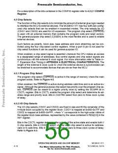
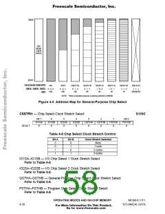
Freescale Semiconductor, Inc.
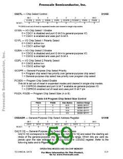
CSCTL — Chip Select Control
$105D
Bit 7
IO1EN
0
6
IO1PL
0
5
IO2EN
0
4
IO2PL
0
3
2
1
PSIZA
0
Bit 0
PSIZB
0
GCSPR PCSEN*
RESET:
0
—
*PCSEN is set out of reset in expanded modes and cleared in single-chip modes.
IO1EN — I/O Chip Select 1 Enable
0 = CSIO1 is disabled and port G bit 5 is general-purpose I/O.
1 = CSIO1 is enabled and uses port G bit 5.
IO1PL — I/O Chip Select 1 Polarity Select
0 = CSIO1 active low
1 = CSIO1 active high
IO2EN — I/O Chip Select 2 Enable
0 = CSIO2 is disabled and port G bit 4 is general-purpose I/O.
1 = CSIO2 is enabled and uses port G bit 4.
IO2PL — I/O Chip Select 2 Polarity Select
0 = CSIO2 active low
1 = CSIO2 active high
GCSPR — General-Purpose Chip Select Priority
0 = Program chip select has priority over general-purpose chip select
1 = General-purpose chip select has priority over program chip select
PCSEN — Program Chip Select Enable
This bit is set out of reset in expanded modes and cleared in single-chip modes.
0 = CSPROG disabled and port G bit 7 available as general-purpose I/O
1 = CSPROG enabled out of reset and uses port G bit 7 pin
PSIZA, PSIZB — Program Chip Select Size (A or B)
Table 4-9 Program Chip Select Size Control
PSIZA
PSIZB
Size (Bytes)
64 K
Address Range
$0000–$FFFF
$8000–$FFFF
$C000–$FFFF
$E000–$FFFF
0
0
1
1
0
1
0
1
32 K
16 K
8 K
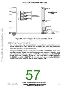
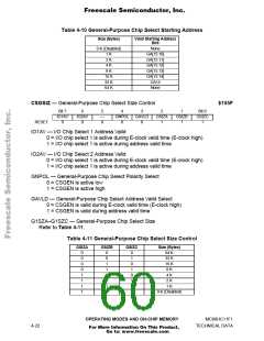
CSGADR — General-Purpose Chip Select Address Register
$105E
Bit 7
GA15
0
6
GA14
0
5
GA13
0
4
GA12
0
3
GA11
0
2
GA10
0
1
—
0
Bit 0
—
RESET:
0
GA[15:10] — General-Purpose Chip Select Base Address
GA[15:10] correspond to MCU address bits ADDR[15:10] and select the starting ad-
dress of the general-purpose chip select's address range. Which bits are valid de-
pends upon the size selected by GSIZA–GSIZC in CSGSIZ register. Refer to the
following table and to Figure 4-4.
OPERATING MODES AND ON-CHIP MEMORY
TECHNICAL DATA
4-21
For More Information On This Product,
Go to: www.freescale.com

 FREESCALE [ Freescale ]