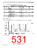
Electrical Characteristics
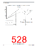
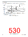
In Figure A-6 the timing diagram for master mode with transmission format CPHA=1 is depicted.
SS
(Output)
1
12
12
13
13
3
2
SCK
(CPOL = 0)
(Output)
4
4
SCK
(CPOL = 1)
(Output)
5
6
MISO
(Input)
Bit MSB-1. . . 1
MSB IN2
LSB IN
11
9
MOSI
(Output)
Port Data
Bit MSB-1. . . 1
Master LSB OUT
Port Data
Master MSB OUT2
1.If configured as output
2. LSBF = 0. For LSBF = 1, bit order is LSB, bit 1,bit 2... MSB.
Figure A-6. SPI Master Timing (CPHA = 1)
S12P-Family Reference Manual, Rev. 1.13
530
Freescale Semiconductor

 FREESCALE [ Freescale ]