Electrical Characteristics
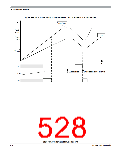
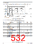
In Figure A-8 the timing diagram for slave mode with transmission format CPHA = 1 is depicted.
SS
(Input)
3
1
12
13
13
2
SCK
(CPOL = 0)
(Input)
4
4
12
11
SCK
(CPOL = 1)
(Input)
8
9
MISO
See
Bit MSB-1 . . . 1
Slave MSB OUT
Slave LSB OUT
LSB IN
Note
(Output)
7
5
6
MOSI
(Input)
MSB IN
Bit MSB-1 . . . 1
NOTE: Not defined
Figure A-8. SPI Slave Timing (CPHA = 1)
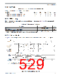
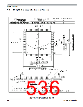
In Table A-28 the timing characteristics for slave mode are listed.
Table A-28. SPI Slave Mode Timing Characteristics
Num
C
Characteristic
SCK frequency
Symbol
Min
Typ
Max
Unit
1
1
D
D
D
D
D
D
D
D
D
D
D
D
D
D
fsck
tsck
tlead
tlag
twsck
tsu
DC
4
—
—
—
—
—
—
—
—
—
—
—
—
—
—
1/4
fbus
tbus
tbus
tbus
tbus
ns
SCK period
∞
2
Enable lead time
4
—
3
Enable lag time
4
—
4
Clock (SCK) high or low time
Data setup time (inputs)
Data hold time (inputs)
Slave access time (time to data active)
Slave MISO disable time
Data valid after SCK edge
Data valid after SS fall
Data hold time (outputs)
Rise and fall time inputs
Rise and fall time outputs
4
—
5
8
—
6
thi
8
—
ns
7
ta
—
—
—
—
20
—
—
20
22
ns
8
tdis
tvsck
tvss
tho
ns
(1)
1
9
29 + 0.5 ⋅ tbus
ns
10
11
12
13
29 + 0.5 ⋅ tbus
ns
—
8
ns
trfi
ns
trfo
8
ns
1. 0.5 tbus added due to internal synchronization delay
S12P-Family Reference Manual, Rev. 1.13
532
Freescale Semiconductor

 FREESCALE [ Freescale ]