Electrical Characteristics
A.10 MSCAN
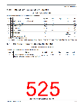
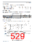
Table A-25. MSCAN Wake-up Pulse Characteristics
Conditions are shown in Table A-4 unless otherwise noted
Num
C
Rating
Symbol
Min
Typ
Max
Unit
1
2
P MSCAN wakeup dominant pulse filtered
P MSCAN wakeup dominant pulse pass
tWUP
tWUP
—
5
—
—
1.5
—
µs
µs
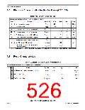
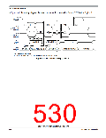
A.11 SPI Timing
This section provides electrical parametrics and ratings for the SPI. In Table A-26 the measurement
conditions are listed.
Table A-26. Measurement Conditions
Description
Value
Unit
Drive mode
Full drive mode
50
—
pF
V
(1)
Load capacitance CLOAD , on all outputs
Thresholds for delay measurement points
(20% / 80%) VDDX
1. Timing specified for equal load on all SPI output pins. Avoid asymmetric load.
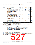
A.11.1 Master Mode
In Figure A-5 the timing diagram for master mode with transmission format CPHA = 0 is depicted.
SS
(Output)
2
1
12
12
13
13
3
SCK
(CPOL = 0)
(Output)
4
4
SCK
(CPOL = 1)
(Output)
5
6
MISO
(Input)
Bit MSB-1. . . 1
9
MSB IN2
10
MSB OUT2
LSB IN
11
MOSI
(Output)
Bit MSB-1. . . 1
LSB OUT
1. If configured as an output.
2. LSBF = 0. For LSBF = 1, bit order is LSB, bit 1, bit 2... MSB.
Figure A-5. SPI Master Timing (CPHA = 0)
S12P-Family Reference Manual, Rev. 1.13
Freescale Semiconductor
529

 FREESCALE [ Freescale ]