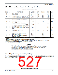
Electrical Characteristics
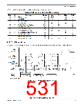
In Table A-27 the timing characteristics for master mode are listed.
Table A-27. SPI Master Mode Timing Characteristics
Num
C
Characteristic
SCK frequency
Symbol
Min
Typ
Max
Unit
1
1
D
D
D
D
D
D
D
D
D
D
D
D
fsck
tsck
tlead
tlag
twsck
tsu
1/2048
2
—
—
1/2
2048
—
fbus
tbus
tsck
tsck
tsck
ns
SCK period
2
Enable lead time
—
—
—
8
1/2
1/2
1/2
—
3
Enable lag time
—
4
Clock (SCK) high or low time
Data setup time (inputs)
Data hold time (inputs)
Data valid after SCK edge
Data valid after SS fall (CPHA = 0)
Data hold time (outputs)
Rise and fall time inputs
Rise and fall time outputs
—
5
—
6
thi
8
—
—
ns
9
tvsck
tvss
tho
—
—
20
—
—
—
29
15
—
ns
10
11
12
13
—
ns
—
ns
trfi
—
8
ns
trfo
—
8
ns
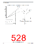
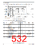
A.11.2 Slave Mode
In Figure A-7 the timing diagram for slave mode with transmission format CPHA = 0 is depicted.
SS
(Input)
1
12
12
13
13
3
SCK
(CPOL = 0)
(Input)
4
4
2
SCK
(CPOL = 1)
10
7
(Input)
8
9
11
11
MISO
(Output)
See
See
Note
Bit MSB-1 . . . 1
Slave LSB OUT
Slave MSB
6
Note
5
MOSI
(Input)
Bit MSB-1. . . 1
MSB IN
LSB IN
NOTE: Not defined
Figure A-7. SPI Slave Timing (CPHA = 0)
S12P-Family Reference Manual, Rev. 1.13
Freescale Semiconductor
531

 FREESCALE [ Freescale ]