Electrical Characteristics
NOTE
All values shown in Table A-19 are preliminary and subject to further
characterization.
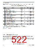
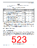
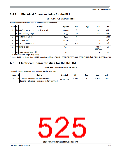
Table A-19. NVM Reliability Characteristics
Conditions are shown in Table A-4 unless otherwise noted
Num
C
Rating
Symbol
Min
Typ
Max
Unit
Program Flash Arrays
1
2
C Data retention at an average junction temperature of TJavg
=
tNVMRET
nFLPE
20
100(2)
—
—
Years
85°C(1) after up to 10,000 program/erase cycles
C Program Flash number of program/erase cycles
10K 100K(3)
Cycles
(-40°C ≤ tj ≤ 150°C)
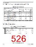
Data Flash Array
3
4
5
6
C Data retention at an average junction temperature of TJavg
=
=
=
tNVMRET
tNVMRET
tNVMRET
nFLPE
5
1002
1002
—
—
—
—
Years
Years
Years
Cycles
85°C1 after up to 50,000 program/erase cycles
C Data retention at an average junction temperature of TJavg
10
85°C1 after up to 10,000 program/erase cycles
C Data retention at an average junction temperature of TJavg
20
1002
85°C1 after less than 100 program/erase cycles
C Data Flash number of program/erase cycles (-40°C ≤ tj ≤ 150°C)
50K
500K3
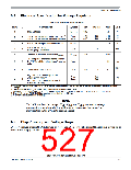
1. TJavg does not exceed 85°C in a typical temperature profile over the lifetime of a consumer, industrial or automotive
application.
2. Typical data retention values are based on intrinsic capability of the technology measured at high temperature and de-rated
to 25°C using the Arrhenius equation. For additional information on how Freescale defines Typical Data Retention, please
refer to Engineering Bulletin EB618
3. Spec table quotes typical endurance evaluated at 25°C for this product family. For additional information on how Freescale
defines Typical Endurance, please refer to Engineering Bulletin EB619.
A.4
Phase Locked Loop
Jitter Definitions
A.4.1
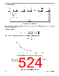
With each transition of the feedback clock, the deviation from the reference clock is measured and input
voltage to the VCO is adjusted accordingly.The adjustment is done continuously with no abrupt changes
in the VCOCLK frequency. Noise, voltage, temperature and other factors cause slight variations in the
control loop resulting in a clock jitter. This jitter affects the real minimum and maximum clock periods as
illustrated in Figure A-2.
S12P-Family Reference Manual, Rev. 1.13
Freescale Semiconductor
523

 FREESCALE [ Freescale ]