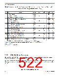
Electrical Characteristics
The D-Flash sector erase time is ~5ms on a new device and can extend to ~20ms as the flash is cycled.
Table A-18. NVM Timing Characteristics (FTMRC)
Num
C
Rating
Symbol
Min
Typ(1)
Max(2)
Unit(3)
1
2
3
4
5
6
7
8
9
Bus frequency
fNVMBUS
fNVMOP
tmass
1
0.8
—
—
—
—
—
—
—
—
—
—
—
—
—
—
—
1.0
100
—
32
1.05
130
35500
130
130
33500
26
MHz
MHz
ms
tcyc
ms
ms
tcyc
ms
µs
Operating frequency
D Erase all blocks (mass erase) time
D Erase verify all blocks (blank check) time
D Unsecure Flash time
tcheck
tuns
100
100
—
D P-Flash block erase time
tpmass
tpcheck
tpera
D P-Flash erase verify (blank check) time
D P-Flash sector erase time
20
D P-Flash phrase programming time
tppgm
226
5(4)
—
285
26
10 D D-Flash sector erase time
tdera
ms
tcyc
µs
11 D D-Flash erase verify (blank check) time
12a D D-Flash one word programming time
12b D D-Flash two word programming time
12c D D-Flash three word programming time
12d D D-Flash four word programming time
tdcheck
tdpgm1
tdpgm2
tdpgm3
tdpgm4
tdpgm4c
2800
107
185
262
339
357
100
170
241
311
328
µs
µs
µs
12e D D-Flash four word programming time crossing row
boundary
µs
1. Typical program and erase times are based on typical fNVMOP and maximum fNVMBUS
2. Maximum program and erase times are based on minimum fNVMOP and maximum fNVMBUS
3. tcyc = 1 / fNVMBUS
4. Typical value for a new device
A.3.2
NVM Reliability Parameters
The reliability of the NVM blocks is guaranteed by stress test during qualification, constant process
monitors and burn-in to screen early life failures.
The data retention and program/erase cycling failure rates are specified at the operating conditions noted.
The program/erase cycle count on the sector is incremented every time a sector or mass erase event is
executed.
S12P-Family Reference Manual, Rev. 1.13
522
Freescale Semiconductor

 FREESCALE [ Freescale ]