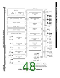
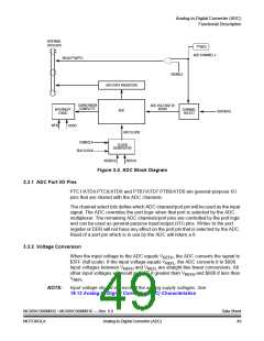
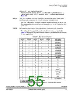
Analog-to-Digital Converter (ADC)
Functional Description
All four of these modes are controlled using MODE0 and MODE1 bits located in
the ADC clock register (ADCR).
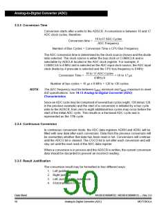
Left justification will place the eight most significant bits (MSB) in the corresponding
ADC data register high, ADRH. This may be useful if the result is to be treated as
an 8-bit result where the two least significant bits (LSB), located in the ADC data
register low, ADRL, can be ignored. However, ADRL must be read after ADRH or
else the interlocking will prevent all new conversions from being stored.
Right justification will place only the two MSBs in the corresponding ADC data
register high, ADRH, and the eight LSBs in ADC data register low, ADRL. This
mode of operation typically is used when a 10-bit unsigned result is desired.
Left justified sign data mode is similar to left justified mode with one exception. The
MSB of the 10-bit result, AD9 located in ADRH, is complemented. This mode of
operation is useful when a result, represented as a signed magnitude from
mid-scale, is needed. Finally, 8-bit truncation mode will place the eight MSBs in
ADC data register low, ADRL. The two LSBs are dropped. This mode of operation
is used when compatibility with 8-bit ADC designs are required. No interlocking
between ADRH and ADRL is present.
NOTE:
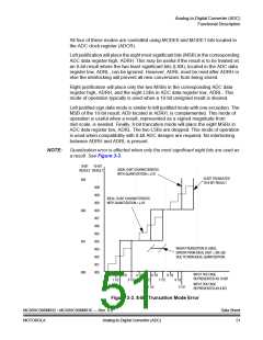
Quantization error is affected when only the most significant eight bits are used as
a result. See Figure 3-3.
8-BIT 10-BIT
IDEAL 8-BIT CHARACTERISTIC
RESULT RESULT
WITH QUANTIZATION = 1/2
10-BIT TRUNCATED
TO 8-BIT RESULT
003
00B
00A
IDEAL 10-BIT CHARACTERISTIC
009
008
007
006
005
004
003
002
001
000
WITH QUANTIZATION = 1/2
002
001
000
WHEN TRUNCATION IS USED,
ERROR FROM IDEAL 8-BIT = 3/8 LSB
DUE TO NON-IDEAL QUANTIZATION.
INPUT VOLTAGE
1/2
2 1/2
4 1/2
6 1/2
8 1/2
REPRESENTED AS 10-BIT
9 1/2
INPUT VOLTAGE
1 1/2
3 1/2
5 1/2
7 1/2
1/2
1 1/2
2 1/2
REPRESENTED AS 8-BIT
Figure 3-3. 8-Bit Truncation Mode Error
MC68HC908MR32 • MC68HC908MR16 — Rev. 6.0
MOTOROLA Analog-to-Digital Converter (ADC)
Data Sheet
51

 FREESCALE [ Freescale ]