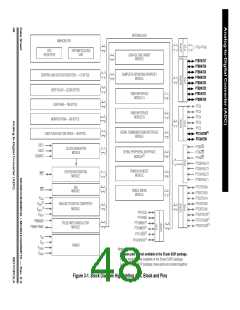
Analog-to-Digital Converter (ADC)
3.3.6 Monotonicity
The conversion process is monotonic and has no missing codes.
3.4 Interrupts
3.5 Wait Mode
When the AIEN bit is set, the ADC module is capable of generating a CPU interrupt
after each ADC conversion. A CPU interrupt is generated if the COCO bit is at 0.
The COCO bit is not used as a conversion complete flag when interrupts are
enabled.
The WAIT instruction can put the MCU in low power-consumption standby mode.
The ADC continues normal operation during wait mode. Any enabled CPU interrupt
request from the ADC can bring the MCU out of wait mode. If the ADC is not
required to bring the MCU out of wait mode, power down the ADC by setting
ADCH[4:0] in the ADC status and control register before executing the WAIT
instruction.
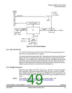
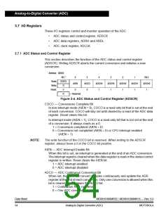
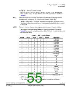
3.6 I/O Signals
The ADC module has 10 input signals that are shared with port B and port C.
3.6.1 ADC Analog Power Pin (VDDAD
)
The ADC analog portion uses VDDAD as its power pin. Connect the VDDAD pin to
the same voltage potential as VDD. External filtering may be necessary to ensure
clean VDDAD for good results.
NOTE:
Route VDDAD carefully for maximum noise immunity and place bypass capacitors
as close as possible to the package.
3.6.2 ADC Analog Ground Pin (VSSAD
)
The ADC analog portion uses VSSAD as its ground pin. Connect the VSSAD pin to
the same voltage potential as VSS.
3.6.3 ADC Voltage Reference Pin (VREFH
)
VREFH is the power supply for setting the reference voltage VREFH. Connect the
VREFH pin to the same voltage potential as VDDAD. There will be a finite current
associated with VREFH. See Section 19. Electrical Specifications.
NOTE:
Route VREFH carefully for maximum noise immunity and place bypass capacitors
as close as possible to the package.
Data Sheet
52
MC68HC908MR32 • MC68HC908MR16 — Rev. 6.0
Analog-to-Digital Converter (ADC)
MOTOROLA

 FREESCALE [ Freescale ]