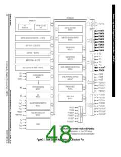
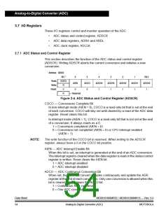
Analog-to-Digital Converter (ADC)
3.3.3 Conversion Time
Conversion starts after a write to the ADSCR. A conversion is between 16 and 17
ADC clock cycles, therefore:
16 to17 ADC Cycles
ADC Frequency
Conversion time =
Number of Bus Cycles = Conversion Time x CPU Bus Frequency
The ADC conversion time is determined by the clock source chosen and the divide
ratio selected. The clock source is either the bus clock or CGMXCLK and is
selectable by ADICLK located in the ADC clock register. For example, if
CGMXCLK is 4 MHz and is selected as the ADC input clock source, the ADC input
clock divide-by-4 prescale is selected and the CPU bus frequency is 8 MHz:
16 to 17 ADC Cycles
Conversion Time =
= 16 to 17 µs
4 MHz/4
Number of bus cycles = 16 µs x 8 MHz = 128 to 136 cycles
NOTE:
The ADC frequency must be between fADIC minimum and fADIC maximum to meet
A/D specifications. See 19.13 Analog-to-Digital Converter (ADC)
Characteristics.
Since an ADC cycle may be comprised of several bus cycles (eight, 136 minus 128,
in the previous example) and the start of a conversion is initiated by a bus cycle
write to the ADSCR, from zero to eight additional bus cycles may occur before the
start of the initial ADC cycle. This results in a fractional ADC cycle and is
represented as the 17th cycle.
3.3.4 Continuous Conversion
In continuous conversion mode, the ADC data registers ADRH and ADRL will be
filled with new data after each conversion. Data from the previous conversion will
be overwritten whether that data has been read or not. Conversions will continue
until the ADCO bit is cleared. The COCO bit is set after each conversion and will
stay set until the next read of the ADC data register.
When a conversion is in process and the ADSCR is written, the current conversion
data should be discarded to prevent an incorrect reading.
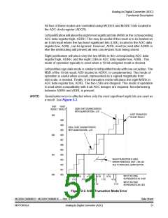
3.3.5 Result Justification
The conversion result may be formatted in four different ways:
1. Left justified
2. Right justified
3. Left Justified sign data mode
4. 8-bit truncation mode
Data Sheet
50
MC68HC908MR32 • MC68HC908MR16 — Rev. 6.0
Analog-to-Digital Converter (ADC) MOTOROLA

 FREESCALE [ Freescale ]