Timer Interface A (TIMA)
Functional Description
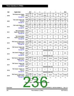
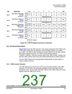
Addr.
Register Name
Bit 7
6
5
4
3
2
1
Bit 0
Read:
TIMA Channel 2 Register High
Bit 15
14
13
12
11
10
9
Bit 8
$001A
(TACH2H) Write:
See page 252.
Reset:
Read:
Indeterminate after reset
TIMA Channel 2 Register Low
Bit 7
6
5
4
3
2
1
Bit 0
$001B
$001C
$001D
$001E
(TACH2L) Write:
See page 252.
Reset:
Read: CH3F
Indeterminate after reset
0
R
0
TIMA Channel 3 Status/Control
See page 249.
CH3IE
MS3A
0
ELS3B
ELS3A
TOV3 CH3MAX
Register (TASC3) Write:
0
0
Reset:
Read:
0
0
0
0
9
0
TIMA Channel 3 Register High
Bit 15
14
13
12
11
10
Bit 8
(TACH3H) Write:
See page 252.
Reset:
Read:
Indeterminate after reset
TIMA Channel 3 Register Low
Bit 7
R
6
5
4
3
2
1
Bit 0
(TACH3L) Write:
See page 252.
Reset:
Indeterminate after reset
= Reserved
Figure 16-3. TIM I/O Register Summary (Continued)
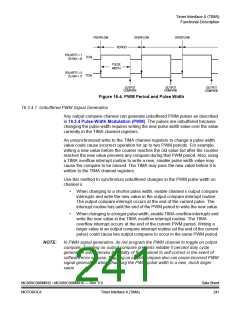
16.3 Functional Description
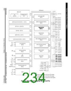
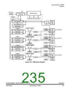
Figure 16-2 shows the TIMA structure. The central component of the TIMA is the
16-bit TIMA counter that can operate as a free-running counter or a modulo
up-counter. The TIMA counter provides the timing reference for the input capture
and output compare functions. The TIMA counter modulo registers,
TAMODH–TAMODL, control the modulo value of the TIMA counter. Software can
read the TIMA counter value at any time without affecting the counting sequence.
The four TIMA channels are programmable independently as input capture or
output compare channels.
16.3.1 TIMA Counter Prescaler
The TIMA clock source can be one of the seven prescaler outputs or the TIMA
clock pin, PTE3/TCLKA. The prescaler generates seven clock rates from the
internal bus clock. The prescaler select bits, PS[2:0], in the TIMA status and control
register select the TIMA clock source.
MC68HC908MR32 • MC68HC908MR16 — Rev. 6.0
MOTOROLA Timer Interface A (TIMA)
Data Sheet
237

 FREESCALE [ Freescale ]