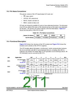
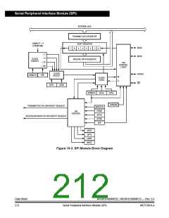
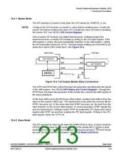
Serial Peripheral Interface Module (SPI)
Transmission Formats
The clock phase (CPHA) control bit selects one of two fundamentally different
transmission formats. The clock phase and polarity should be identical for the
master SPI device and the communicating slave device. In some cases, the phase
and polarity are changed between transmissions to allow a master device to
communicate with peripheral slaves having different requirements.
NOTE:
Before writing to the CPOL bit or the CPHA bit, disable the SPI by clearing the SPI
enable bit (SPE).
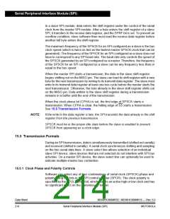
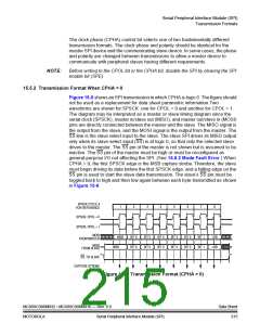
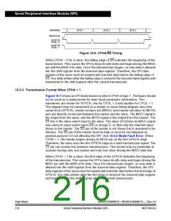
15.5.2 Transmission Format When CPHA = 0
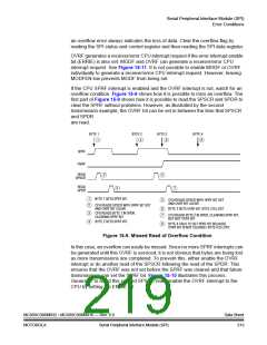
Figure 15-5 shows an SPI transmission in which CPHA is logic 0. The figure should
not be used as a replacement for data sheet parametric information.Two
waveforms are shown for SPSCK: one for CPOL = 0 and another for CPOL = 1.
The diagram may be interpreted as a master or slave timing diagram since the
serial clock (SPSCK), master in/slave out (MISO), and master out/slave in (MOSI)
pins are directly connected between the master and the slave. The MISO signal is
the output from the slave, and the MOSI signal is the output from the master. The
SS line is the slave select input to the slave. The slave SPI drives its MISO output
only when its slave select input (SS) is at logic 0, so that only the selected slave
drives to the master. The SS pin of the master is not shown but is assumed to be
inactive. The SS pin of the master must be high or must be reconfigured as
general-purpose I/O not affecting the SPI. (See 15.6.2 Mode Fault Error.) When
CPHA = 0, the first SPSCK edge is the MSB capture strobe. Therefore, the slave
must begin driving its data before the first SPSCK edge, and a falling edge on the
SS pin is used to start the slave data transmission. The slave’s SS pin must be
toggled back to high and then low again between each byte transmitted as shown
in Figure 15-6.
SPSCK CYCLE #
FOR REFERENCE
1
2
3
4
5
6
7
8
SPSCK, CPOL = 0
SPSCK, CPOL = 1
MOSI
FROM MASTER
MSB
BIT 6
BIT 6
BIT 5
BIT 5
BIT 4
BIT 4
BIT 3
BIT 3
BIT 2
BIT 2
BIT 1
BIT 1
LSB
LSB
MISO
FROM SLAVE
MSB
SS, TO SLAVE
CAPTURE STROBE
Figure 15-5. Transmission Format (CPHA = 0)
MC68HC908MR32 • MC68HC908MR16 — Rev. 6.0
MOTOROLA Serial Peripheral Interface Module (SPI)
Data Sheet
215

 FREESCALE [ Freescale ]