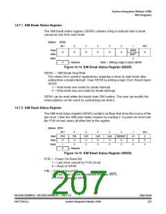
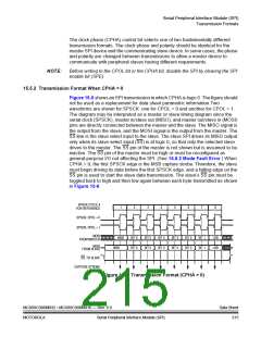
Serial Peripheral Interface Module (SPI)
Pin Name Conventions
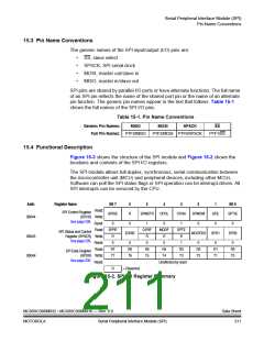
15.3 Pin Name Conventions
The generic names of the SPI input/output (I/O) pins are:
•
•
•
•
SS, slave select
SPSCK, SPI serial clock
MOSI, master out/slave in
MISO, master in/slave out
SPI pins are shared by parallel I/O ports or have alternate functions. The full name
of an SPI pin reflects the name of the shared port pin or the name of an alternate
pin function. The generic pin names appear in the text that follows. Table 15-1
shows the full names of the SPI I/O pins.
Table 15-1. Pin Name Conventions
Generic Pin Names:
MISO
MOSI
SPSCK
SS
Full Pin Names: PTF3/MISO
PTF2/MOSI PTF0/SPSCK
PTF1/SS
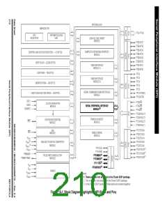
15.4 Functional Description
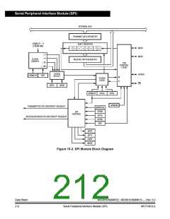
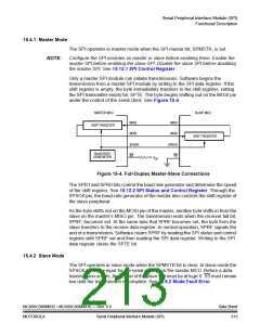
Figure 15-3 shows the structure of the SPI module and Figure 15-2 shows the
locations and contents of the SPI I/O registers.
The SPI module allows full-duplex, synchronous, serial communication between
the microcontroller unit (MCU) and peripheral devices, including other MCUs.
Software can poll the SPI status flags or SPI operation can be interrupt-driven. All
SPI interrupts can be serviced by the CPU.
Addr.
Register Name
Bit 7
SPRIE
0
6
5
4
3
2
1
SPE
0
Bit 0
SPTIE
0
Read:
SPI Control Register
(SPCR) Write:
See page 228.
R
0
SPMSTR
CPOL
CPHA
SPWOM
0
$0044
Reset:
1
OVRF
R
0
MODF
R
1
SPTE
R
Read: SPRF
SPI Status and Control
See page 229.
ERRIE
MODFEN
SPR1
SPR0
$0045
$0046
Register (SPSCR) Write:
R
0
Reset:
Read:
0
0
0
1
0
0
0
R7
T7
R6
T6
R5
T5
R4
T4
R3
T3
R2
T2
R1
T1
R0
T0
SPI Data Register
(SPDR) Write:
See page 232.
Reset:
Unaffected by reset
R
= Reserved
Figure 15-2. SPI I/O Register Summary
MC68HC908MR32 • MC68HC908MR16 — Rev. 6.0
MOTOROLA Serial Peripheral Interface Module (SPI)
Data Sheet
211

 FREESCALE [ Freescale ]