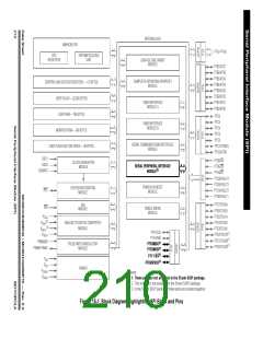
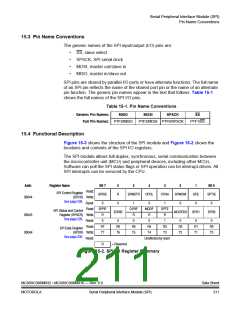
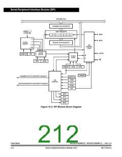
Serial Peripheral Interface Module (SPI)
In a slave SPI module, data enters the shift register under the control of the serial
clock from the master SPI module. After a byte enters the shift register of a slave
SPI, it transfers to the receive data register, and the SPRF bit is set. To prevent an
overflow condition, slave software then must read the receive data register before
another full byte enters the shift register.
The maximum frequency of the SPSCK for an SPI configured as a slave is the bus
clock speed (which is twice as fast as the fastest master SPSCK clock that can be
generated). The frequency of the SPSCK for an SPI configured as a slave does not
have to correspond to any SPI baud rate. The baud rate only controls the speed of
the SPSCK generated by an SPI configured as a master. Therefore, the frequency
of the SPSCK for an SPI configured as a slave can be any frequency less than or
equal to the bus speed.
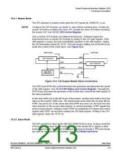
When the master SPI starts a transmission, the data in the slave shift register
begins shifting out on the MISO pin. The slave can load its shift register with a new
byte for the next transmission by writing to its transmit data register. The slave must
write to its transmit data register at least one bus cycle before the master starts the
next transmission. Otherwise, the byte already in the slave shift register shifts out
on the MISO pin. Data written to the slave shift register during a transmission
remains in a buffer until the end of the transmission.
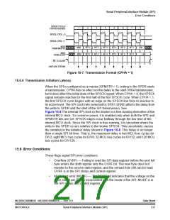
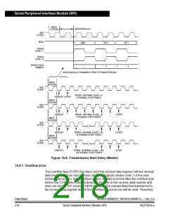
When the clock phase bit (CPHA) is set, the first edge of SPSCK starts a
transmission. When CPHA is clear, the falling edge of SS starts a transmission.
See 15.5 Transmission Formats.
NOTE:
If the write to the data register is late, the SPI transmits the data already in the shift
register from the previous transmission.
SPSCK must be in the proper idle state before the slave is enabled to prevent
SPSCK from appearing as a clock edge.
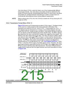
15.5 Transmission Formats
During an SPI transmission, data is simultaneously transmitted (shifted out serially)
and received (shifted in serially). A serial clock synchronizes shifting and sampling
on the two serial data lines. A slave select line allows selection of an individual
slave SPI device; slave devices that are not selected do not interfere with SPI bus
activities. On a master SPI device, the slave select line can optionally be used to
indicate multiple-master bus contention.
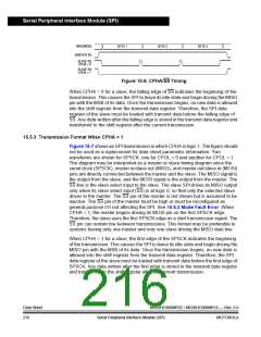
15.5.1 Clock Phase and Polarity Controls
Software can select any of four combinations of serial clock (SPSCK) phase and
polarity using two bits in the SPI control register (SPCR). The clock polarity is
specified by the CPOL control bit, which selects an active high or low clock and has
no significant effect on the transmission format.
Data Sheet
214
MC68HC908MR32 • MC68HC908MR16 — Rev. 6.0
Serial Peripheral Interface Module (SPI)
MOTOROLA

 FREESCALE [ Freescale ]