Serial Communications Interface Module (SCI)
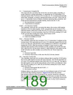
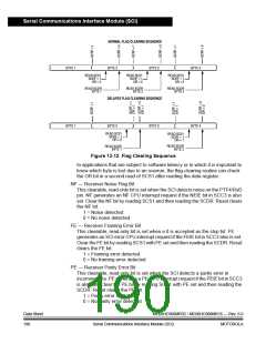
NORMAL FLAG CLEARING SEQUENCE
BYTE 1
BYTE 2
BYTE 3
BYTE 4
READ SCS1
SCRF = 1
OR = 0
READ SCS1
SCRF = 1
OR = 0
READ SCS1
SCRF = 1
OR = 0
READ SCDR
BYTE 1
READ SCDR
BYTE 2
READ SCDR
BYTE 3
DELAYED FLAG CLEARING SEQUENCE
BYTE 1
BYTE 2
BYTE 3
BYTE 4
READ SCS1
SCRF = 1
OR = 0
READ SCS1
SCRF = 1
OR = 1
READ SCDR
BYTE 1
READ SCDR
BYTE 3
Figure 13-12. Flag Clearing Sequence
In applications that are subject to software latency or in which it is important to
know which byte is lost due to an overrun, the flag-clearing routine can check
the OR bit in a second read of SCS1 after reading the data register.
NF — Receiver Noise Flag Bit
This clearable, read-only bit is set when the SCI detects noise on the PTF4/RxD
pin. NF generates an NF CPU interrupt request if the NEIE bit in SCC3 is also
set. Clear the NF bit by reading SCS1 and then reading the SCDR. Reset clears
the NF bit.
1 = Noise detected
0 = No noise detected
FE — Receiver Framing Error Bit
This clearable, read-only bit is set when a 0 is accepted as the stop bit. FE
generates an SCI error CPU interrupt request if the FEIE bit in SCC3 also is set.
Clear the FE bit by reading SCS1 with FE set and then reading the SCDR. Reset
clears the FE bit.
1 = Framing error detected
0 = No framing error detected
PE — Receiver Parity Error Bit
This clearable, read-only bit is set when the SCI detects a parity error in
incoming data. PE generates a PE CPU interrupt request if the PEIE bit in SCC3
is also set. Clear the PE bit by reading SCS1 with PE set and then reading the
SCDR. Reset clears the PE bit.
1 = Parity error detected
0 = No parity error detected
Data Sheet
190
MC68HC908MR32 • MC68HC908MR16 — Rev. 6.0
Serial Communications Interface Module (SCI)
MOTOROLA

 FREESCALE [ Freescale ]