Pulse-Width Modulator for Motor Control (PWMMC)
Fault Protection
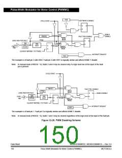
BIT 7
DISABLE
PWM PIN 1
BIT 6
BIT 5
DISABLE
PWM PIN 2
DISABLE
PWM PIN 3
BIT 4
BIT 3
BANK X
DISABLE
BANK Y
DISABLE
DISABLE
PWM PIN 4
BIT 2
DISABLE
PWM PIN 5
BIT 1
BIT 0
DISABLE
PWM PIN 6
Figure 12-27. PWM Disabling Decode Scheme
12.6.1.1 Fault Pin Filter
Each fault pin incorporates a filter to assist in determining a genuine fault condition.
After a fault pin has been logic low for one CPU cycle, a rising edge (logic high) will
be synchronously sampled once per CPU cycle for two cycles. If both samples are
detected logic high, the corresponding FPIN bit and FFLAG bit will be set. The
FPIN bit will remain set until the corresponding fault pin is logic low and
synchronously sampled once in the following CPU cycle.
12.6.1.2 Automatic Mode
In automatic mode, the PWM(s) are disabled immediately once a filtered fault
condition is detected (logic high). The PWM(s) remain disabled until the filtered
fault condition is cleared (logic low) and a new PWM cycle begins as shown in
Figure 12-28. Clearing the corresponding FFLAGx event bit will not enable the
PWMs in automatic mode.
MC68HC908MR32 • MC68HC908MR16 — Rev. 6.0
MOTOROLA Pulse-Width Modulator for Motor Control (PWMMC)
Data Sheet
151

 FREESCALE [ Freescale ]