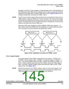
Pulse-Width Modulator for Motor Control (PWMMC)
Fault Protection
12.6 Fault Protection
Conditions may arise in the external drive circuitry which require that the PWM
signals become inactive immediately, such as an overcurrent fault condition.
Furthermore, it may be desirable to selectively disable PWM(s) solely with
software.
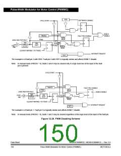
One or more PWM pins can be disabled (forced to their inactive state) by applying
a logic high to any of the four external fault pins or by writing a logic high to either
of the disable bits (DISX and DISY in PWM control register 1). Figure 12-26 shows
the structure of the PWM disabling scheme. While the PWM pins are disabled, they
are forced to their inactive state. The PWM generator continues to run — only the
output pins are disabled.
To allow for different motor configurations and the controlling of more than one
motor, the PWM disabling function is organized as two banks, bank X and bank Y.
Bank information combines with information from the disable mapping register to
allow selective PWM disabling. Fault pin 1, fault pin 2, and PWM disable bit X
constitute the disabling function of bank X. Fault pin 3, fault pin 4, and PWM disable
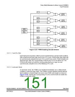
bit Y constitute the disabling function of bank Y. Figure 12-25 and Figure 12-27
show the disable mapping write-once register and the decoding scheme of the
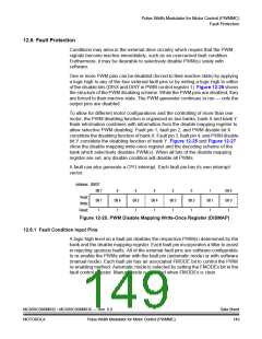
bank which selectively disables PWM(s). When all bits of the disable mapping
register are set, any disable condition will disable all PWMs.
A fault can also generate a CPU interrupt. Each fault pin has its own interrupt
vector.
Address: $0037
Bit 7
Bit 7
1
6
Bit 6
1
5
Bit 5
1
4
Bit 4
1
3
Bit 3
1
2
Bit 2
1
1
Bit 1
1
Bit 0
Bit 0
1
Read:
Write:
Reset:
Figure 12-25. PWM Disable Mapping Write-Once Register (DISMAP)
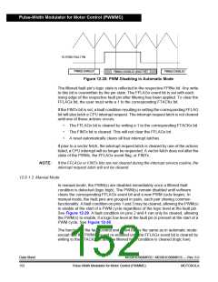
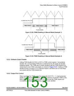
12.6.1 Fault Condition Input Pins
A logic high level on a fault pin disables the respective PWM(s) determined by the
bank and the disable mapping register. Each fault pin incorporates a filter to assist
in rejecting spurious faults. All of the external fault pins are software-configurable
to re-enable the PWMs either with the fault pin (automatic mode) or with software
(manual mode). Each fault pin has an associated FMODE bit to control the PWM
re-enabling method. Automatic mode is selected by setting the FMODEx bit in the
fault control register. Manual mode is selected when FMODEx is clear.
MC68HC908MR32 • MC68HC908MR16 — Rev. 6.0
MOTOROLA Pulse-Width Modulator for Motor Control (PWMMC)
Data Sheet
149

 FREESCALE [ Freescale ]