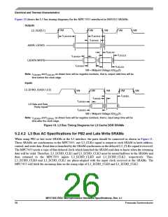
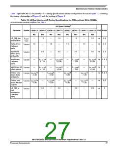
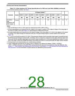
Electrical and Thermal Characteristics
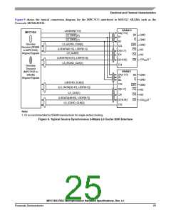
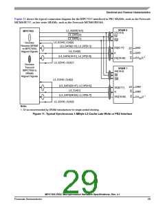
Figure 9 shows the typical connection diagram for the MPC7455 interfaced to MSUG2 SRAMs such as the
Freescale MCM64E836.
SRAM 0
L3ADDR[17:0]
MPC7455
SA[17:0]
B3 GND
L3_CNTL[0]
B1
G
GND
L3_CNTL[1]
B2
Denotes
L3_ECHO_CLK[0]
LBO GND
CQ
Receive (SRAM
to MPC7455)
Aligned Signals
{L3DATA[0:15], L3DP[0:1]}
L3_CLK[0]
CQ
CQ
CK
NC
NC
D[0:17]
CK
{L3DATA[16:31], L3DP[2:3]}
L3_ECHO_CLK[1]
1
GV /2
D[18:35]
CQ
DD
Denotes
Transmit
SRAM 1
SA[17:0]
B1
(MPC7455 to
SRAM)
Aligned Signals
B3 GND
G
GND
LBO GND
B2
L3ECHO_CLK[2]
CQ
{L3_DATA[32:47],L3DP[4:5]}
D[0:17]
CQ
CQ
CK
NC
NC
L3_CLK[1]
CK
{L3DATA[48:63], L3DP[6:7]}
L3_ECHO_CLK[3]
1
D[18:35]
CQ
GV /2
DD
Note:
1. Or as recommended by SRAM manufacturer for single-ended clocking.
Figure 9. Typical Source Synchronous 2-Mbyte L3 Cache DDR Interface
MPC7455 RISC Microprocessor Hardware Specifications, Rev. 4.1
Freescale Semiconductor
25

 FREESCALE [ Freescale ]