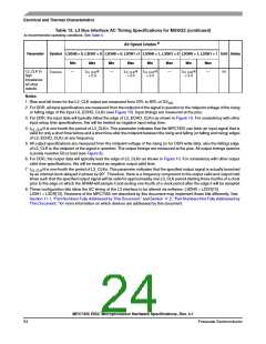
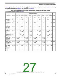
Electrical and Thermal Characteristics
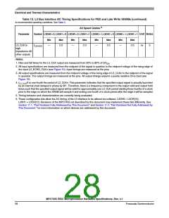
Table 13. L3 Bus Interface AC Timing Specifications for PB2 and Late Write SRAMs (continued)
At recommended operating conditions. See Table 4.
6
All Speed Grades
Parameter
Symbol
Unit Notes
L3OH0 = 0, L3OH1 = 0 L3OH0 = 0, L3OH1 =1 L3OH0 = 1, L3OH1 = 0 L3OH0 = 1, L3OH1 = 1
Min
Max
Min
Max
Min
Max
Min
Max
L3_CLK to
high
t
—
2.0
—
2.0
—
2.0
—
2.0
ns
5
L3CHOZ
impedance:All
other outputs
Notes:
1. Rise and fall times for the L3_CLK output are measured from 20% to 80% of GV
.
DD
2. All input specifications are measured from the midpoint of the signal in question to the midpoint voltage of the rising edge of
the input L3_ECHO_CLKn (see Figure 10). Input timings are measured at the pins.
3. All output specifications are measured from the midpoint voltage of the rising edge of L3_CLKn to the midpoint of the signal
in question. The output timings are measured at the pins. All output timings assume a purely resistive 50-Ω load (see
Figure 10).
4. t
/4 is one-fourth the period of L3_CLKn. This parameter indicates that the specified output signal is actually launched
L3_CLK
by an internal clock delayed in phase by 90°. Therefore, there is a frequency component to the output valid and output hold
times such that the specified output signal will be valid for approximately one L3_CLK period starting three-fourths of a clock
prior to the edge on which the SRAM will sample it and ending one-fourth of a clock period after the edge it will be sampled.
5. Timing behavior and characterization are currently being evaluated.
6. These configuration bits allow the AC timing of the L3 interface to be altered via software. L3OH0 = L2CR[12],
L30H1 = L3CR[12]. Revisions of the MPC7455 not described by this document may implement these bits differently. See
Section 11.1, “Part Numbers Fully Addressed by This Document,” and Section 11.2, “Part Numbers Not Fully Addressed by
This Document,” for more information on which devices are addressed by this document.
MPC7455 RISC Microprocessor Hardware Specifications, Rev. 4.1
28
Freescale Semiconductor

 FREESCALE [ Freescale ]