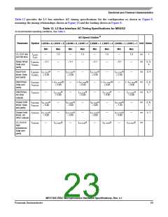
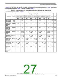
Electrical and Thermal Characteristics
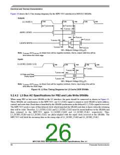
Table 13 provides the L3 bus interface AC timing specifications for the configuration shown in Figure 11, assuming
the timing relationships of Figure 12 and the loading of Figure 8.
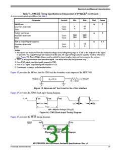
Table 13. L3 Bus Interface AC Timing Specifications for PB2 and Late Write SRAMs
At recommended operating conditions. See Table 4.
6
All Speed Grades
Parameter
Symbol
L3OH0 = 0, L3OH1 = 0 L3OH0 = 0, L3OH1 =1 L3OH0 = 1, L3OH1 = 0 L3OH0 = 1, L3OH1 = 1
Unit Notes
Min
Max
Min
Max
Min
Max
Min
Max
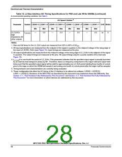
L3_CLK rise
and fall time
t
t
,
—
1.0
—
1.0
—
1.0
—
1.0
ns
ns
1, 5
2, 5
L3CR
L3CF
Setup times:
Data and
parity
t
t
1.5
—
—
—
—
1.5
—
—
1.5
—
—
1.5
—
—
L3DVEH
L3DXEH
L3CHDV
L3CHOV
Input hold
times: Data
and parity
0.5
0.5
0.5
0.5
ns
2, 5
Valid times:
Data and
parity
t
t
t
/4
—
t
t
/4
—
t
t
/4
—
t
/4 ns 3, 4, 5
L3_CLK
+ 0.40
L3_CLK
+ 1.00
L3_CLK
+ 0.80
L3_CLK
+ 0.60
Valid times: All
other outputs
t
/4
—
/4
—
/4
—
t
/4 ns
4
L3_CLK
+ 1.00
L3_CLK
+ 0.80
L3_CLK
+ 0.60
L3_CLK
+ 0.40
Output hold
times: Data
and parity
t
t
/4
– 0.40
—
t
t
/4
– 0.60
—
t
t
/4
– 0.80
—
t
t
/4
– 1.00
—
ns 3, 4, 5
L3CHDX L3_CLK
L3_CLK
L3_CLK
L3_CLK
Output hold
times:Allother
outputs
t
t
/4
– 0.40
—
/4
—
/4
—
/4
—
ns
ns
4, 5
5
L3CHOX L3_CLK
L3_CLK
L3_CLK
L3_CLK
– 0.60
– 0.80
– 1.00
L3_CLK to
high
t
—
2.0
—
2.0
—
2.0
—
2.0
L3CHDZ
impedance:
Data and
parity
MPC7455 RISC Microprocessor Hardware Specifications, Rev. 4.1
Freescale Semiconductor
27

 FREESCALE [ Freescale ]