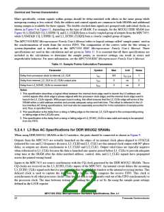
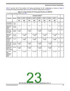
Electrical and Thermal Characteristics
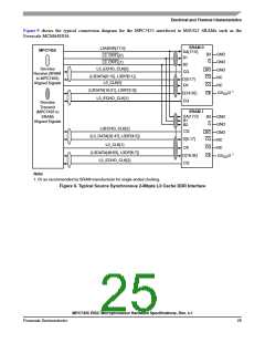
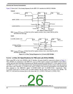
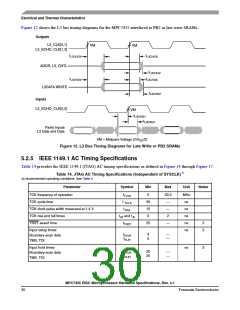
Figure 10 shows the L3 bus timing diagrams for the MPC7455 interfaced to MSUG2 SRAMs.
Outputs
VM
VM
VM
VM
VM
L3_CLK[0,1]
ADDR, L3CNTL
L3DATA WRITE
t
t
L3CHOZ
L3CHOV
t
L3CHOX
t
L3CLDV
t
L3CLDZ
t
L3CHDV
t
L3CHDX
t
L3CLDX
VM = Midpoint Voltage (GV /2)
DD
Note: t
and t
as drawn here will be negative numbers, that is, output valid time will be
L3CLDV
L3CHDV
time before the clock edge.
Inputs
L3_ECHO_CLK[0,1,2,3]
VM
VM
VM
VM
VM
t
L3DXEL
t
L3DVEL
t
t
L3DVEH
L3 Data and Data
Parity Inputs
L3DXEH
VM = Midpoint Voltage (GV /2)
DD
Note: t
and t
as drawn here will be negative numbers, that is, input setup time will be
L3DVEH
L3DVEL
time after the clock edge.
Figure 10. L3 Bus Timing Diagrams for L3 Cache DDR SRAMs
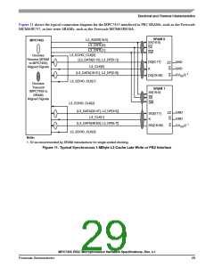
5.2.4.2 L3 Bus AC Specifications for PB2 and Late Write SRAMs
When using PB2 or late write SRAMs at the L3 interface, the parts should be connected as shown in Figure 11.
These SRAMs are synchronous to the MPC7455; one L3_CLKn signal is output to each SRAM to latch address,
control, and write data. Read data is launched by the SRAM synchronous to the delayed L3_CLKn signal it received.
The MPC7455 needs a copy of that delayed clock which launched the SRAM read data to know when the returning
data will be valid. Therefore, L3_ECHO_CLK1 and L3_ECHO_CLK3 must be routed halfway to the SRAMs and
then returned to the MPC7455 inputs L3_ECHO_CLK0 and L3_ECHO_CLK2, respectively. Thus,
L3_ECHO_CLK0 and L3_ECHO_CLK2 are phase-aligned with the input clock received at the SRAMs. The
MPC7455 will latch the incoming data on the rising edge of L3_ECHO_CLK0 and L3_ECHO_CLK2.
MPC7455 RISC Microprocessor Hardware Specifications, Rev. 4.1
26
Freescale Semiconductor

 FREESCALE [ Freescale ]