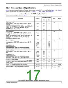
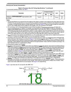
Electrical and Thermal Characteristics
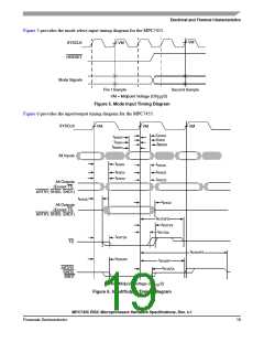
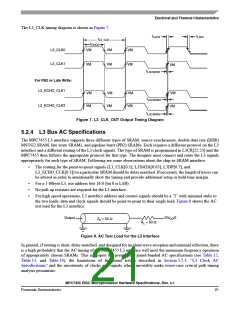
The L3_CLK timing diagram is shown in Figure 7.
t
t
L3CF
L3CR
t
L3_CLK
t
CHCL
L3_CLK0
L3_CLK1
VM
VM
VM
VM
VM
VM
VM
t
L3CSKW1
For PB2 or Late Write:
L3_ECHO_CLK1
VM
VM
VM
VM
VM
VM
VM
VM
t
L3CSKW2
L3_ECHO_CLK3
t
L3CSKW2
Figure 7. L3_CLK_OUT Output Timing Diagram
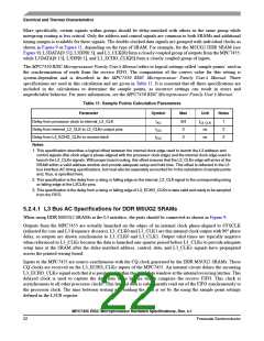
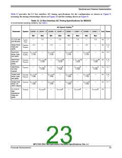
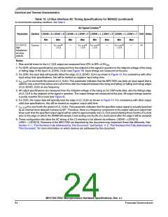
5.2.4 L3 Bus AC Specifications
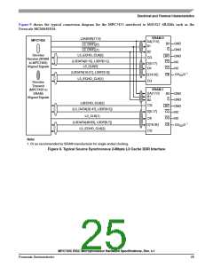
The MPC7455 L3 interface supports three different types of SRAM: source-synchronous, double data rate (DDR)
MSUG2 SRAM, late write SRAMs, and pipeline burst (PB2) SRAMs. Each requires a different protocol on the L3
interface and a different routing of the L3 clock signals. The type of SRAM is programmed in L3CR[22:23] and the
MPC7455 then follows the appropriate protocol for that type. The designer must connect and route the L3 signals
appropriately for each type of SRAM. Following are some observations about the chip-to-SRAM interface.
•
The routing for the point-to-point signals (L3_CLK[0:1], L3DATA[0:63], L3DP[0:7], and
L3_ECHO_CLK[0:3]) to a particular SRAM should be delay matched. If necessary, the length of traces can
be altered in order to intentionally skew the timing and provide additional setup or hold time margin.
•
•
•
For a 1-Mbyte L3, use address bits 16:0 (bit 0 is LSB).
No pull-up resistors are required for the L3 interface.
For high speed operations, L3 interface address and control signals should be a ‘T’ with minimal stubs to
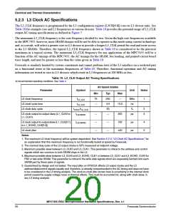
the two loads; data and clock signals should be point-to-point to their single load. Figure 8 shows the AC
test load for the L3 interface.
Output
GV /2
DD
Z = 50 Ω
0
R = 50 Ω
L
Figure 8. AC Test Load for the L3 Interface
In general, if routing is short, delay-matched, and designed for incident wave reception and minimal reflection, there
is a high probability that the AC timing of the MPC7455 L3 interface will meet the maximum frequency operation
of appropriately chosen SRAMs. This is despite the pessimistic, guard-banded AC specifications (see Table 12,
Table 13, and Table 14), the limitations of functional testers described in Section 5.2.3, “L3 Clock AC
Specifications,” and the uncertainty of clocks and signals which inevitably make worst-case critical path timing
analysis pessimistic.
MPC7455 RISC Microprocessor Hardware Specifications, Rev. 4.1
Freescale Semiconductor
21

 FREESCALE [ Freescale ]