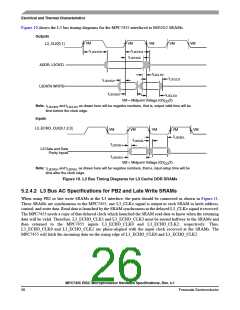
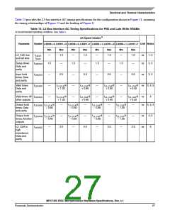
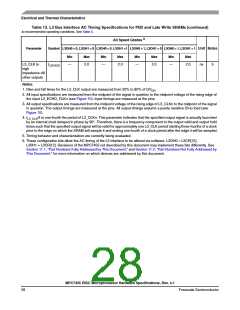
Electrical and Thermal Characteristics
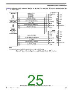
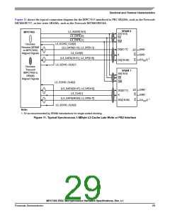
Figure 11 shows the typical connection diagram for the MPC7455 interfaced to PB2 SRAMs, such as the Freescale
MCM63R737, or late write SRAMs, such as the Freescale MCM63R836A.
SRAM 0
SA[16:0]
L3_ADDR[16:0]
L3_CNTL[0]
L3_CNTL[1]
MPC7455
SS
SW
L3_ECHO_CLK[0]
Denotes
Receive (SRAM
to MPC7455)
Aligned Signals
{L3_DATA[0:15], L3_DP[0:1]}
DQ[0:17]
GND
GND
ZZ
G
L3_CLK[0]
K
{L3_DATA[16:31], L3_DP[2:3]}
1
GV /2
DQ[18:36]
K
DD
L3_ECHO_CLK[1]
L3_ECHO_CLK[2]
Denotes
Transmit
(MPC7455 to
SRAM)
SRAM 1
SA[16:0]
SS
Aligned Signals
SW
{L3_DATA[32:47], L3_DP[4:5]}
L3_CLK[1]
GND
GND
ZZ
G
DQ[0:17]
K
{L3_DATA[48:63], L3_DP[6:7]}
1
DQ[18:36]
K
GV /2
DD
L3_ECHO_CLK[3]
Note:
1. Or as recommended by SRAM manufacturer for single-ended clocking.
Figure 11. Typical Synchronous 1-MByte L3 Cache Late Write or PB2 Interface
MPC7455 RISC Microprocessor Hardware Specifications, Rev. 4.1
Freescale Semiconductor
29

 FREESCALE [ Freescale ]