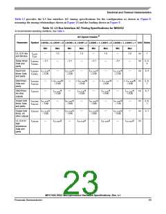
Electrical and Thermal Characteristics
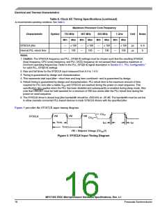
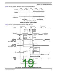
Figure 5 provides the mode select input timing diagram for the MPC7455.
VM
VM
SYSCLK
HRESET
Mode Signals
Firs t Sample
Second Sample
VM = Midpoint Voltage (OV /2)
DD
Figure 5. Mode Input Timing Diagram
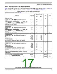
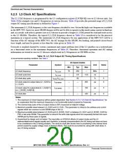
Figure 6 provides the input/output timing diagram for the MPC7455.
SYSCLK
VM
VM
VM
t
t
t
AXKH
IXKH
t
t
AVKH
IVKH
MXKH
t
MVKH
All Inputs
t
t
KHAV
KHAX
KHDX
KHOX
t
t
t
t
KHDV
KHOV
All Outputs
(Except TS,
ARTRY, SHD0, SHD1)
t
KHOE
tKHOZ
All Outputs
(Except TS,
ARTRY, SHD0, SHD1)
tKHTSPZ
t
KHTSV
t
KHTSX
tKHTSV
TS
tKHARPZ
tKHARV
tKHARP
ARTRY,
SHD0,
SHD1
tKHARX
VM = Midpoint Voltage (OV /2)
DD
Figure 6. Input/Output Timing Diagram
MPC7455 RISC Microprocessor Hardware Specifications, Rev. 4.1
Freescale Semiconductor
19

 FREESCALE [ Freescale ]