Freescale Semiconductor, Inc.
Timing System
Pulse-width modulation (PWM) timer
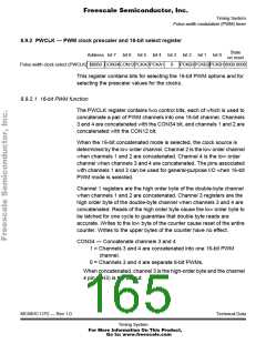
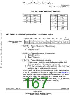
Table 8-4. Clock A and clock B prescalers
PCKA[2:1]
Clock A
E
PCKB[3:1]
0 0 0
Clock B
E
0 0
0 1
1 0
1 1
E/2
0 0 1
E/2
E/4
0 1 0
E/4
E/8
0 1 1
E/8
1 0 0
E/16
E/32
E/64
E/128
1 0 1
1 1 0
1 1 1
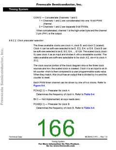
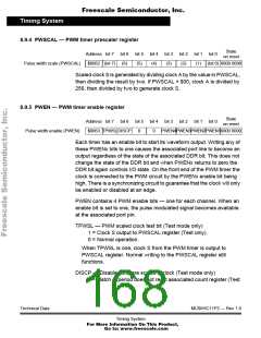
8.9.3 PWPOL — PWM timer polarity & clock source select register
State
on reset
Address bit 7 bit 6 bit 5 bit 4 bit 3 bit 2 bit 1 bit 0
Pulse width polarity select
(PWPOL)
$0061 PCLK4 PCLK3 PCLK2 PCLK1 PPOL4PPOL3PPOL2PPOL10000 0000
PCLK[4:3] — Pulse width channel 4/3 clock select
1 = Clock S is source.
0 = Clock B is source.
PCLK[2:1] — Pulse width channel 2/1 clock select
1 = Clock S is source.
0 = Clock A is source.
PPOL[4:1] — Pulse width channel x polarity
1 = PWM channel x output is high at the beginning of the clock
cycle and goes low when duty count is reached.
0 = PWM channel x output is low at the beginning of the clock cycle
and goes high when duty count is reached.
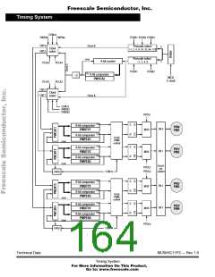
Each channel has a polarity bit that allows a cycle to start with either
a high or a low level. This is shown on the block diagram, Figure 8-4,
as a selection of either the Q output or the Q output of the PWM output
flip flop. When one of the bits in the PWPOL register is set, the
associated PWM channel output is high at the beginning of the clock
cycle, then goes low when the duty count is reached.
MC68HC11P2 — Rev 1.0
Technical Data
Timing System
For More Information On This Product,
Go to: www.freescale.com

 FREESCALE [ Freescale ]