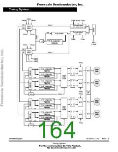
Freescale Semiconductor, Inc.
Timing System
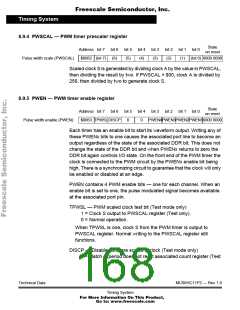
8.9.4 PWSCAL — PWM timer prescaler register
State
on reset
Address bit 7 bit 6 bit 5 bit 4 bit 3 bit 2 bit 1 bit 0
$0062 (bit 7) (6) (5) (4) (3) (2)
Pulse width scale (PWSCAL)
(1) (bit 0) 0000 0000
Scaled clock S is generated by dividing clock A by the value in PWSCAL,
then dividing the result by two. If PWSCAL = $00, clock A is divided by
256, then divided by two to generate clock S.
8.9.5 PWEN — PWM timer enable register
State
on reset
Address bit 7 bit 6 bit 5 bit 4 bit 3 bit 2 bit 1 bit 0
Pulse width enable (PWEN)
$0063 TPWSLDISCP PWEN4PWEN3PWEN2PWEN10000 0000
0
0
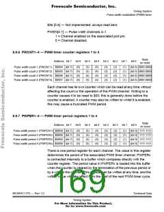
Each timer has an enable bit to start its waveform output. Writing any of
these PWENx bits to one causes the associated port line to become an
output regardless of the state of the associated DDR bit. This does not
change the state of the DDR bit and when PWENx returns to zero the
DDR bit again controls I/O state. On the front end of the PWM timer the
clock is connected to the PWM circuit by the PWENx enable bit being
high. There is a synchronizing circuit to guarantee that the clock will only
be enabled or disabled at an edge.
PWEN contains 4 PWM enable bits — one for each channel. When an
enable bit is set to one, the pulse modulated signal becomes available
at the associated port pin.
TPWSL — PWM scaled clock test bit (Test mode only)
1 = Clock S output to PWSCAL register (Test only).
0 = Normal operation.
When TPWSL is one, clock S from the PWM timer is output to
PWSCAL register. Normal writing to the PWSCAL register still
functions.
DISCP — Disable compare scaled E clock (Test mode only)
1 = Match of period does not reset associated count register (Test
Technical Data
MC68HC11P2 — Rev 1.0
Timing System
For More Information On This Product,
Go to: www.freescale.com

 FREESCALE [ Freescale ]