Freescale Semiconductor, Inc.
Timing System
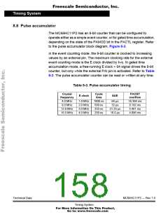
Pulse accumulator
TOF
RTIF
PAOVF
PAIF
1
&
L
0
0
0
0
TOI
RTII
PAOVI
PAII
0
T
Interrupt
requests
g
2
&
n
i
2
t
t
s
a
l
MT
0
E/64 clock
(from main timer)
PR1
PR0
&
Overflow
Enable
2:1
MUX
Clock
PACNT
PA7/
OC1/
PAI
Input buffer
and edge detector
Output buffer
From
OC1
PACTL
From
DDRA7
Internal data bus
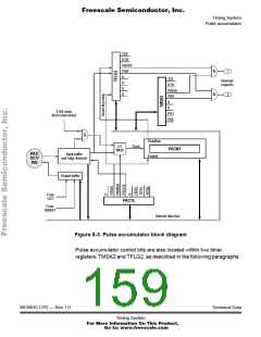
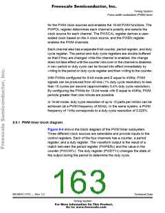
Figure 8-3. Pulse accumulator block diagram
Pulse accumulator control bits are also located within two timer
registers, TMSK2 and TFLG2, as described in the following paragraphs.
MC68HC11P2 — Rev 1.0
Technical Data
Timing System
For More Information On This Product,
Go to: www.freescale.com

 FREESCALE [ Freescale ]