FUNCTIONAL DEVICE OPERATION
RESET AND WATCHDOG PINS, SOFTWARE WATCHDOG OPERATIONS
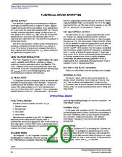
the MCU to enter its low power mode, a deglitcher time of
typical 40 µs is implemented.
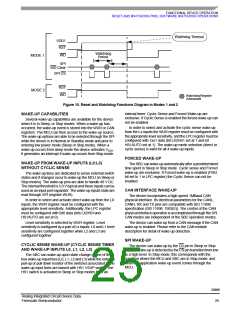
Figure 9 indicates the operation to enter Stop mode.
SPI Stop/ Sleep Command
SPI CS
tCSSTOP
I
DD1DGLT
SBC in Stop mode
with IDD1over I wake-up
SBC in Stop mode
no IDD1 over I wake-up
SBC in Normal or Stand-by mode
Figure 9. Operation Entering Stop Mode
RESET AND WATCHDOG PINS, SOFTWARE WATCHDOG OPERATIONS
SOFTWARE WATCHDOG (SELECTABLE WINDOW
RESET PIN DESCRIPTION
OR TIMEOUT WATCHDOG)
A reset output is necessary and available to reset the
microcontroller. Modes 1 and 2 are available for the reset pin
(please refer to Table 5 for reset pin operation).
Software watchdog uses in the SBC Normal and Standby
modes is to monitor MCU. The Watchdog can be either
window or timeout. This is selectable by SPI (register TIM1,
bit WDW). Default is window watchdog. The period for the
watchdog is selectable from the SPI from 10 ms to 350 ms
(register TIM1, bits WDT0 and WDT1). When the window
watchdog is selected, the closed window is the first part of the
selected period, and the open window is the second part of
the period. Refer to the SPI TIM register description.
Watchdog can only be cleared within the open window time.
An attempt to clear the watchdog in the closed window will
generate a reset. Watchdog is cleared through SPI by
addressing the TIM1 register.
Reset causes when SBC is in mode 1:
• VDD1 falling out of range — If VDD1 falls below the reset
threshold (parameter RSTTH), the ret pin is pulled low until
VDD1 returns to the normal voltage.
• Power-on reset — At device power-on or at device wake-
up from Sleep mode, the reset is maintained low until VDD1
is within its operation range.
Watchdog timeout — If watchdog is not cleared, the SBC
will pull the reset pin low for the duration of the reset time
(parameter RSTDUR)
.
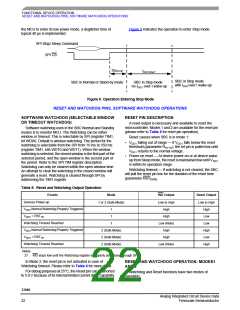
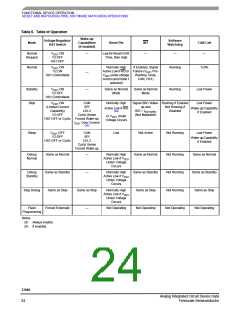
Table 5. Reset and Watchdog Output Operation
Events
Devices Power-up
Mode
WD Output
Reset Output
1 or 2 (Safe Mode)
Low to High
High
Low to High
High
VDD1 Normal Watchdog Properly Triggered
VDD1 < RSTTH
1
1
High
Low
Watchdog Timeout Reached
VDD1 Normal Watchdog Properly Triggered
VDD1 < RSTTH
1
Low (Note)
High
Low
2 (Safe Mode)
2 (Safe Mode)
2 (Safe Mode)
High
High
Low
Watchdog Timeout Reached
Low (Note)
High
Notes
27. WD stays low until the Watchdog register is properly addressed through SPI.
In Mode 2, the reset pin is not activated in case of
Watchdog timeout. Please refer to Table 6 for more detail.
RESET AND WATCHDOG OPERATION: MODES1
AND 2
For debug purposes at 25°C, the Reset pin can be shorted
to 5.0 V because of its internal limited current drive capability.
Watchdog and Reset functions have two modes of
operation:
33989
Analog Integrated Circuit Device Data
Freescale Semiconductor
22

 FREESCALE [ Freescale ]