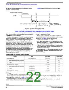
FUNCTIONAL DESCRIPTION
INTRODUCTION
FUNCTIONAL DESCRIPTION
INTRODUCTION
The 33989 is an integrated circuit dedicated to automotive
applications. Its functions include:
• Driver for an external path transistor for the V2 regulator
function
• Reset, programmable watchdog function, interrupt, and
four operational modes
• One full protected voltage regulator with 200 mA total
output current capability available at VDD1 external pin
• Programmable wake-up input and Cyclic Sense wake-up
• CAN high-speed physical interface
FUNCTIONAL PIN DESCRIPTION
connect V2 to an external 5.0 V regulator or to the VDD1
output when no external series pass transistor is used. In this
case, the V2CTRL pin must be left open.
RECEIVE AND TRANSMIT DATA (RXD AND TXD)
The RX and TX pins (receive data and transmit data pins,
respectively) are connected to a microcontroller’s CAN
protocol handler. TXD is an input and controls the CANH and
CANL line state (dominant when TXD is LOW, recessive
when TXD is HIGH). RXD is an output and reports the bus
state (RXD LOW when CAN bus is dominant, HIGH when
CAN bus is recessive).
VOLTAGE SOURCE 2 CONTROL (V2CTRL)
The V2CTRL pin is the output drive pin for the V2 regulator
connected to the external series pass transistor.
VOLTAGE SUPPLY (VSUP)
VOLTAGE DIGITAL DRAIN ONE (VDD1)
The VSUP pin is the battery supply input of the device.
The VDD1 pin is the output pin of the 5.0 V internal
regulator. It can deliver up to 200 mA. This output is protected
against overcurrent and overtemperature. It includes an
overtemperature pre-warning flag, which is set when the
internal regulator temperature exceeds 130°C typical. When
the temperature exceeds the overtemperature shutdown
(170°C typical), the regulator is turned off.
HIGH-SIDE ONE (HS1)
The HS1 pin is the internal high-side driver output. It is
internally protected against overcurrent and
overtemperature.
LEVEL 0-3 INPUTS (L0:L3)
VDD1 includes an undervoltage reset circuitry, which sets
the RST pin LOW when VDD1 is below the undervoltage reset
threshold.
The L0:L3 pins can be connected to contact switches or
the output of other ICs for external inputs. The input states
can be read by SPI. These inputs can be used as wake-up
events for the SBC when operating in the Sleep or Stop
mode.
RESET (RST)
The Reset pin RST is an output that is set LOW when the
device is in reset mode. The RST pin is set HIGH when the
device is not in reset mode. RST includes an internal pullup
current source. When RST is LOW, the sink current capability
is limited, allowing RST to be shorted to 5.0 V for software
debug or software download purposes.
CAN HIGH AND CAN LOW OUTPUTS
(CANH AND CANL)
The CAN High and CAN Low pins are the interfaces to the
CAN bus lines. They are controlled by TX input level, and the
state of CANH and CANL is reported through RX output. A
60 Ω termination resistor is connected between CANH and
CANL pins.
INTERRUPT (INT)
The Interrupt pin INT is an output that is set LOW when an
interrupt occurs. INT is enabled using the Interrupt Register
(INTR). When an interrupt occurs, INT stays LOW until the
interrupt source is cleared.
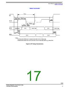
SYSTEM CLOCK (SCLK)
SCLK is the System Clock input pin of the serial peripheral
interface.
INT output also reports a wake-up event by a 10 µs typical
pulse when the device is in Stop mode.
MASTER IN SLAVE OUT (MISO)
MISO is the Master In Slave Out pin of the serial peripheral
interface. Data is sent from the SBC to the microcontroller
through the MISO pin.
VOLTAGE SOURCE TWO (V2)
The V2 pin is the input sense for the V2 regulator. It is
connected to the external series pass transistor. V2 is also
the 5.0 V supply of the internal CAN interface. It is possible to
33989
Analog Integrated Circuit Device Data
Freescale Semiconductor
18

 FREESCALE [ Freescale ]